
By Aveek Sarkar, Director, Ecosystem and Alliance Management Division, TSMC
September 24, 2026
As the global semiconductor industry races to meet the insatiable demands of artificial intelligence, TSMC is taking decisive steps to streamline how advanced chips are designed, validated, and manufactured. In a wide-ranging discussion on the evolution of the foundry’s Open Innovation Platform (OIP) Ecosystem, Aveek Sarkar, director of ecosystem and alliance management at TSMC, shared the company’s forward-looking vision for enabling AI-driven agentic workflows. Central to this strategy is the introduction of the new TSMC AI Design Kit (ADK), a transformative toolset designed to accelerate time-to-market and dramatically boost engineering productivity across digital, analog, and radio frequency (RF) design domains.
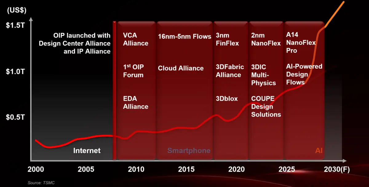
The genesis of TSMC’s OIP ecosystem lies in the maturation of the pure-play foundry model, which fundamentally democratized silicon innovation for companies of all sizes. Over nearly two decades since its formal establishment, the OIP has expanded into a formidable collaborative network encompassing more than 90 members across six distinct alliances, featuring over 100,000 intellectual property (IP) blocks and comprehensive reference flows. According to Sarkar, the core mission of this collaborative framework remains straightforward: streamlining the customer design process, accelerating development schedules, and de-risking every step of the journey from initial concept to successful tape-out and commercial revenue generation.

Today, this collaborative network is widely recognized as a leadership ecosystem, but Sarkar emphasizes that true leadership requires looking around corners to anticipate the future needs of customers. To address these emerging demands, TSMC is actively supporting startups focused on AI-based electronic design automation (EDA) and specialized AI IP integration. Furthermore, the company is broadening its scope beyond traditional silicon and advanced packaging to encompass a system-level focus at the rack level. This initiative aims to assist original design manufacturers (ODMs) who may operate outside the traditional OIP framework but remain critical components of the broader customer ecosystem.
Energy Efficiency Remains the Paramount Challenge for AI Infrastructure
Amid the rapid expansion of artificial intelligence, energy efficiency has emerged as the single most critical challenge facing the entire technology sector. TSMC and its extensive network of OIP partners are tackling this hurdle through a multi-pronged approach centered on compute efficiency, heterogeneous integration with advanced memory, and high-performance connectivity.
In the realm of compute, TSMC relies heavily on design technology co-optimization (DTCO), an approach that develops circuit-level IP and underlying process technologies in tandem to extract the maximum potential benefits in power, performance, and area (PPA). However, technological readiness is only half the battle. To ensure customers can successfully leverage these innovations, TSMC collaborates closely with ecosystem partners, design service providers, and value chain alliances to deploy robust design flows and offer hands-on support. In addition to digital compute, the foundry places a major emphasis on analog circuit optimization, working with partners from the earliest stages of process design kit (PDK) development to refine analog PPA metrics, which are vital for managing power consumption in I/O circuits.

At the system level, advanced packaging technologies such as TSMC-SoIC (system-on-integrated chips) enable 3D chiplet stacking, though they introduce complex multi-physics challenges including thermal management and mechanical stress. Addressing these factors requires deep ecosystem collaboration, ensuring that designers have the tools necessary to manage these physical phenomena effectively.
Meanwhile, connectivity is being revolutionized by TSMC COUPE, a breakthrough technology that requires the simultaneous optimization of electrical and optical components. Achieving high-fidelity electromagnetic extraction and managing the thermal properties that directly impact performance necessitate rigorous modeling across the entire system hierarchy, extending from individual packages up to entire server racks and Internet of Things (IoT) platforms.
Transforming Design Productivity with the AI Design Kit
As artificial intelligence workloads grow increasingly complex, the adoption of AI within design tools themselves has accelerated. To capitalize on this trend, TSMC is introducing the AI Design Kit (ADK), an initiative engineered to speed up time-to-market by enabling agentic AI-based design tools and workflows built upon TSMC-specific technology learning.

The deployment of the TSMC ADK is projected to yield staggering productivity gains, boosting digital design efficiency by three to five times and increasing analog and RF design productivity by up to six times. While traditional reference flows have long enabled customers to achieve strong results, they frequently require manual tuning and workflow optimization tailored to specific project requirements. Moving forward, agentic frameworks are expected to automate and accelerate these circuit- and architecture-specific optimizations.
Unlike conventional reference flows governed by static conditions, the TSMC ADK injects a foundational layer of technology-specific knowledge directly into the agentic framework. This empowers AI agents to tune designs optimally and hit targeted metrics with unprecedented speed. Although TSMC expects to gather valuable insights through ongoing customer engagement, the foundational framework is positioned to drive rapid industry progress. This builds upon years of foundational work in reinforcement learning applied to circuit optimization and design space exploration, including methodologies that facilitate smooth design migration between different process nodes.
Addressing Power and Cost at the Edge versus the Cloud
While hyperscale data centers command much of the attention in the AI era, the expansion of AI workloads to edge computing introduces distinct priorities centered around energy efficiency and cost containment. Customer trends for edge silicon are increasingly gravitating toward FinFET nodes to capture substantial power advantages.

Through the deployment of ultra-low leakage SRAM, edge devices can maintain minimal standby power consumption while accommodating larger memory capacities or operating at reduced voltages to significantly lower dynamic power usage. Ecosystem partners play a critical role in this domain by ensuring customers have ready access to application-tuned IP libraries. A notable example of this collaboration involves an IP Alliance partner working alongside customer Ambiq to develop custom IP solutions on TSMC’s N12e process, achieving dramatic leakage power reductions tailored for edge AI applications.
Real-World Success Driven by Ecosystem Collaboration
The tangible impact of TSMC’s OIP ecosystem was prominently showcased at the recent North America OIP Forum. Greg Dix, vice president of engineering for the ASIC Product Division at Broadcom, highlighted how his team leverages TSMC’s leading-edge technologies and robust design ecosystem to construct custom XPU platforms at scale. Broadcom’s success in adopting advanced nodes, executing heterogeneous multi-die integration, and implementing near-memory co-design exemplifies the power of collaborative silicon development.
Furthermore, TSMC has engaged in extensive joint validation projects with major memory providers, including SK hynix, Samsung Memory, and Micron, focusing on HBM5 CoWoS (Chip-on-Wafer-on-Substrate) integration and best practices for mitigating thermal-mechanical stress. By partnering with leading EDA vendors, TSMC has also organized advanced training programs for the design services community, lowering barriers to entry and helping customers de-risk their path to production.

Looking to the Future of the Leadership Ecosystem
As the semiconductor industry navigates ongoing technological transitions, the OIP ecosystem continues to adapt to new paradigms. Engineers are increasingly moving beyond single-step AI applications toward orchestrated workflows where multiple intelligent agents collaborate and share insights throughout the design cycle. Because these agents operate continuously, they dramatically shorten the feedback loops associated with timing, parasitics, and thermal analysis, opening the door for hardware-accelerated engines and customized large language models capable of predicting complex design tradeoffs.
Simultaneously, TSMC is aggressively expanding its focus into system-level engineering, looking beyond silicon and packaging to address the holistic requirements of data centers, humanoid robots, and IoT infrastructure in close alignment with its ODM partners. Through continued collaboration and pioneering initiatives like the AI Design Kit, TSMC and its ecosystem partners are laying a solid foundation for the next generation of intelligent silicon innovation.



Leave a Reply