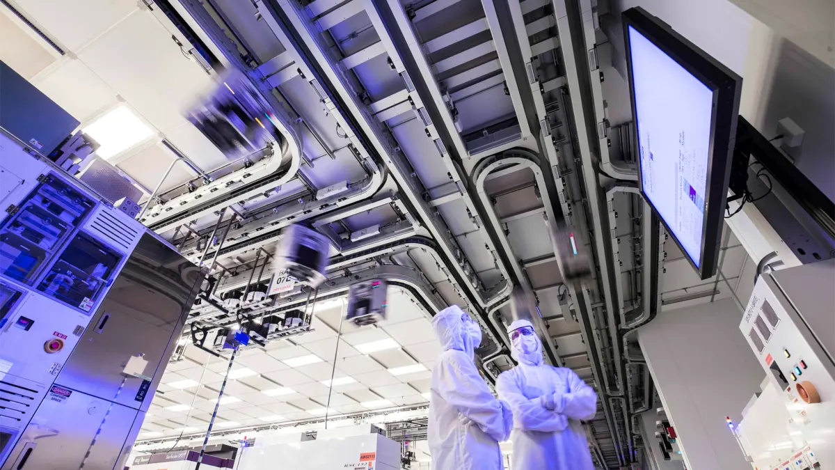
GlobalFoundries is setting its sights on the next decade of semiconductor manufacturing with an ambitious roadmap for its proprietary manufacturing techniques. A company vice president has provided detailed insights into the development of FDX Fusion technology, a promising manufacturing approach designed to deliver 7nm-class performance levels entirely without the use of extreme ultraviolet (EUV) lithography tools. With high-volume manufacturing targeted for the year 2030, the foundry is positioning this upcoming node as a strategic alternative for clients seeking advanced performance characteristics without the immense capital expenditure typically required by cutting-edge EUV-reliant nodes.
The core premise behind the FDX Fusion initiative centers on leveraging established, cost-effective lithography equipment while still achieving performance metrics traditionally associated with much denser, bleeding-edge manufacturing nodes. According to the executive briefing, the technology relies on planar transistors rather than moving to more complex 3D architectures like FinFET or Gate-All-Around (GAA) transistors that dominate the sub-7nm landscape. By sticking with planar designs, GlobalFoundries aims to bypass some of the manufacturing bottlenecks and exorbitant tooling costs that have become standard in modern semiconductor fabrication.
However, achieving 7nm-class performance with planar transistors comes with distinct engineering trade-offs. The most notable characteristic of the upcoming FDX Fusion process is its low transistor density compared to standard commercial 7nm nodes offered by industry giants using EUV scanners. While the raw density may be lower, the technology is designed to compensate by delivering strong operational efficiency, favorable power profiles, and specific performance advantages tailored to targeted workloads where extreme transistor packing is secondary to thermal management, cost efficiency, and specialized electrical characteristics.
The decision to avoid EUV tools is a significant part of GlobalFoundries’ broader strategy. Extreme ultraviolet lithography systems, manufactured almost exclusively by ASML, represent some of the most expensive machinery in the world, often costing hundreds of millions of dollars per unit. By circumventing the need for these tools, GlobalFoundries can potentially maintain a more flexible cost structure, mitigating some of the financial risks associated with building out advanced fabrication capacity. This approach could prove particularly attractive to designers of automotive chips, Internet of Things (IoT) devices, and specialized processors that require robust performance scaling without bearing the financial burden of mainstream smartphone- or PC-grade nodes.
The timeline shared by the company places the push toward high-volume manufacturing around 2030. This gives the engineering teams several years to refine the FDX Fusion platform, optimize the planar transistor architecture, and ensure that the process can achieve the desired yields at scale. Foundry customers and industry observers will be watching closely as development continues, eager to see how a non-EUV, planar approach can effectively compete in an ecosystem where denser 3D transistor architectures have become the baseline standard for high-performance computing.
As the semiconductor industry navigates rising manufacturing costs and complex supply chain dynamics, alternative pathways like GlobalFoundries’ FDX Fusion highlight the diverse strategies being deployed to keep performance scaling viable. By targeting a 2030 window for high-volume production, the company is staking out a distinct long-term vision—one that seeks to bridge the gap between advanced-node performance and the economic pragmatism of non-EUV manufacturing.