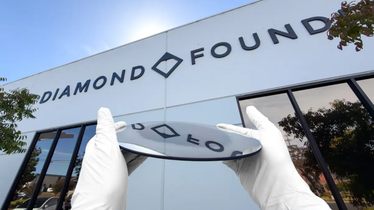
Diamonds have long been celebrated for their brilliance and rarity in the world of jewelry, but their exceptional physical properties have increasingly captured the attention of the technology and semiconductor industries. Among these remarkable attributes is an extraordinary capacity for cooling, driven by a level of thermal conductivity that makes diamond at least five times more conductive than copper, the traditional benchmark for heat management in electronics. Capitalizing on this physical marvel, lab-grown diamond specialist Diamond Foundry has announced the creation of the world’s first 200mm single-crystal diamond (SCD) wafer, marking a monumental shift in how advanced computing hardware might manage extreme thermal loads in the future.
The introduction of the 200mm single-crystal diamond wafer represents a major milestone because it matches the standard wafer sizes traditionally utilized by semiconductor fabrication plants for older, yet still widely deployed, manufacturing processes. By scaling up single-crystal diamond to this industrial dimension, Diamond Foundry is signaling that the material has successfully transitioned from a boutique laboratory curiosity into a viable medium for commercial semiconductor manufacturing. Proclaiming on its official corporate website that "single-crystal diamond has entered the wafer-scale era," the company is positioning its proprietary technology as a direct response to the escalating thermal crises facing modern data centers, high-performance computing clusters, and particularly the rapidly expanding artificial intelligence hardware sector.
The timing of this development is far from coincidental. In recent years, the semiconductor industry has collided with a formidable wall of physics: as processing power has scaled upward to meet the immense computational demands of artificial intelligence, machine learning, and deep neural network training, the amount of heat generated by these silicon behemoths has skyrocketed. Modern AI accelerators and processors consume unprecedented amounts of electrical power, which in turn converts into massive quantities of thermal energy. Traditional cooling methodologies—ranging from standard aluminum and copper heatsinks to complex liquid cooling loops and vapor chambers—are rapidly approaching their physical limits when tasked with dissipating the concentrated heat fluxes produced by cutting-edge processors.
This is where the unique atomic structure of diamond offers a revolutionary alternative. Pure diamond consists of a rigid, tightly bound lattice of carbon atoms held together by strong covalent bonds. This atomic configuration allows phonons—quasiparticles that represent vibrational waves—to travel through the material with exceptionally low scattering resistance. Because thermal conductivity in non-metallic solids is primarily mediated by phonon transport, diamond’s pristine crystal lattice facilitates the rapid and efficient transfer of thermal energy away from hot spots. When compared against copper, which relies on the movement of free electrons to conduct heat, diamond’s phonon-mediated thermal conductivity outpaces it by a factor of five or more, making it arguably the most efficient natural thermal conductor known to science.
However, harnessing this capability has historically been hindered by the immense difficulty of manufacturing diamond at scale, particularly in the form of large, uniform single crystals. Naturally occurring diamonds are rare, unpredictable in size, and cost-prohibitive for industrial engineering applications. Even within the realm of synthetic or lab-grown diamonds, producing polycrystalline diamond films has been common for industrial cutting tools and basic heat spreaders, but these materials suffer from grain boundaries that scatter phonons and reduce overall thermal efficiency. Single-crystal diamond, by contrast, eliminates these grain boundaries entirely, offering uninterrupted thermal pathways that maximize the material’s cooling potential.
Diamond Foundry’s breakthrough in producing a 200mm single-crystal diamond wafer directly addresses the long-standing manufacturing bottleneck that has kept diamond out of mainstream semiconductor pipelines. For decades, researchers and engineers recognized that integrating diamond into microelectronic packaging could theoretically solve chronic overheating issues in high-power electronics, radio frequency amplifiers, and power semiconductors. Yet, the inability to grow these crystals in sizes compatible with existing semiconductor fabrication equipment meant that diamond components had to be painstakingly cut, shaped, and applied in small, fragmented patches rather than integrated seamlessly at the wafer level.
By achieving a 200mm diameter for a single-crystal diamond wafer, Diamond Foundry has bridged the gap between advanced materials science and commercial semiconductor manufacturing infrastructure. Fabrication plants around the world are tooled to handle wafers of standardized dimensions, allowing automated machinery to transport, etch, deposit, and process the materials with high precision. While leading-edge semiconductor nodes have largely transitioned to 300mm wafers, a 200mm standard remains entirely relevant for many power electronics, specialized processors, and mature process technologies where thermal management is often the primary performance-limiting factor rather than transistor density alone.
The broader implications for the tech industry are profound, especially as designers of high-performance processors grapple with thermal design power (TDP) ratings that continue to climb into the hundreds of watts per single chip. When processors run too hot, manufacturers are forced to implement thermal throttling, a protective mechanism that intentionally slows down clock speeds to prevent physical damage to the silicon. This throttling directly degrades performance, undermining the very gains that engineers work tirelessly to achieve with each new microarchitecture generation. By utilizing diamond-based cooling solutions derived from wafer-scale production, the industry could theoretically bypass these thermal bottlenecks, allowing AI chips and high-performance processors to sustain peak computational performance indefinitely without running the risk of thermal degradation or catastrophic failure.
As Diamond Foundry continues its efforts to manufacture single-crystal diamond at commercial scale, the integration of these wafers into the semiconductor supply chain will depend on how effectively the material can be processed, bonded, and scaled alongside traditional silicon and advanced packaging substrates. The company’s recent announcement serves as a clear indication that the material science required to tackle next-generation thermal challenges is maturing rapidly. With artificial intelligence workloads projected to demand even greater computational density in the years ahead, the successful rollout of wafer-scale single-crystal diamond could fundamentally transform how the technology industry approaches cooling and power management in the most demanding computing environments.