
By Dr. Jim Shiely, Technical and strategic advisor, Siemens EDA
September 30, 2026
Better hardware enables better software, and in turn, better software enables better hardware. The modern semiconductor industry operates entirely inside this accelerating feedback loop, generating unprecedented volumes of simulation results, metrology data, and manufacturing evidence. Yet, as information becomes increasingly abundant across the ecosystem, the industry’s primary bottleneck is shifting decisively from information generation to rapid, high-stakes decision-making.
The next major competitive advantage for semiconductor manufacturers will not come from simply generating more information or collecting larger datasets. Instead, it will come from learning what truly matters in the manufacturing process and acting on it faster than the competition. Overcoming this hurdle requires an emerging and distinct discipline: Manufacturing Intelligence.
Beyond Information: The New Bottleneck
For most of the historical evolution of semiconductor manufacturing, progress depended heavily on the industry’s sheer ability to generate better information. When a specific engineering problem became too difficult to solve with existing methods, teams responded by building a more sophisticated simulation model or deploying a more sensitive metrology system.
That concerted effort succeeded remarkably well. Today, engineers can accurately simulate complex semiconductor devices before they even exist physically, and they can collect fab measurements at an unimaginable scale across production lines.
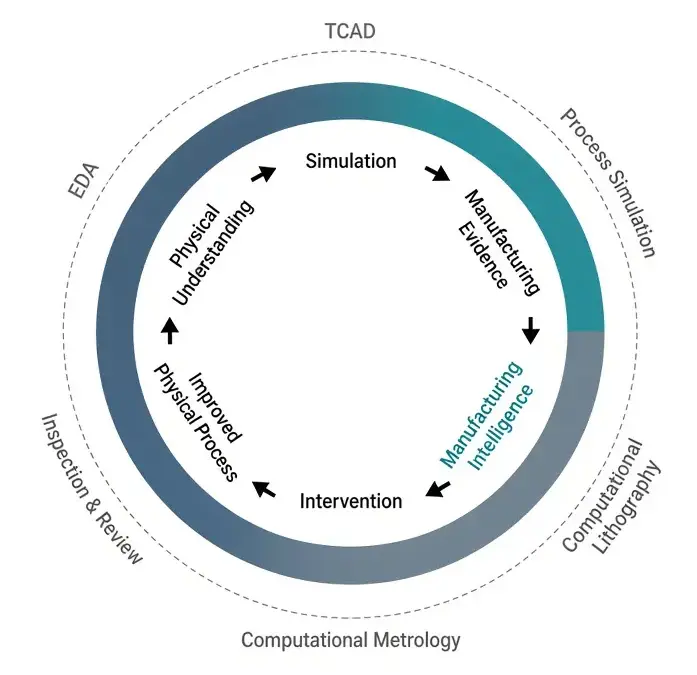
However, manufacturing yield does not improve simply because massive amounts of data exist in a server repository. Manufacturing outcomes improve exclusively when information directly changes a decision on the floor. Manufacturing Intelligence represents the systematic conversion of underlying physical understanding and granular manufacturing observations into trusted interventions that actively improve final outcomes.
Electronic design automation (EDA) occupies a uniquely strategic position within this ecosystem. While most software applications merely benefit from better hardware performance, EDA actually helps create the better hardware, which then turns around and supports the next generation of EDA software. EDA actively participates in both directions of the critical hardware-software feedback loop, helping to determine how quickly the underlying computing platform can evolve.

From Prediction to Intervention
Historically, simulation, metrology, and optimization were treated as completely separate silos within semiconductor fabrication and design flows. Rising manufacturing complexity, however, is rapidly eroding those traditional boundaries. As process windows continue to narrow, prediction and observation can no longer operate as independent, disconnected activities.
The stark distinction between mere information and meaningful action explains why certain technologies create disproportionate value in the market. A computer simulation alone does not change a physical process; a metrology measurement alone does not improve a device. Even the most accurate prediction creates zero value until someone changes something in the manufacturing process in direct response to it.
Computational lithography provides a mature and proven blueprint for this approach. Optical proximity correction (OPC) and inverse lithography (ILT) sit precisely at the critical intersection of physical understanding, manufacturing observation, and corrective action. The ultimate output of these advanced systems is not just another analytical report to file away; it is a direct intervention in the manufacturing process, applied seamlessly across full-chip designs at full production scale. The ultimate purpose of intelligence is not mere prediction, but informed action.
Physics and Measurement: A Single Conversation
The economic value of any individual measurement depends heavily on its ability to improve an underlying model, while the value of a model depends entirely on how effectively it explains real-world measurements. Neither domain is sufficient on its own.
A purely physics-based approach quickly encounters material and process uncertainties that are simply too complex to model completely from first principles. On the other hand, a purely measurement-driven approach observes what happened after the fact, but it cannot necessarily explain why it happened or accurately predict what will happen next time.
Manufacturing Intelligence emerges organically from the continuous interaction between these two distinct perspectives. Simulation organizes exploration by identifying sensitivities and directing engineering attention where it matters most, while metrology grounds those theoretical models firmly in physical reality. Computational metrology, alongside advanced manufacturing inspection and review systems, extends that vital relationship by converting complex contours, microscopic images, defects, and process-variation trends into actionable evidence within a larger representation.
This comprehensive representation combines physical models, historical manufacturing data, and deep engineering knowledge. As a result, measurement no longer stands apart from modeling; each continuously improves the other in a closed-loop learning system.

The Rules of Industrial AI
In high-stakes semiconductor manufacturing, machine learning operates under radically different rules compared to consumer applications or enterprise software.
First and foremost, Manufacturing Intelligence must remain strictly accountable to physical reality. The objective is never merely to produce a plausible answer, but rather to deliver an outcome that is completely consistent with physical laws. Statistical intelligence and machine learning models cannot be permitted to invent a fabricated reality that the underlying physical system cannot possibly support.
Second, industrial manufacturing requires absolute stability and predictability. While a consumer-facing chatbot or recommendation engine can answer the exact same user prompt differently tomorrow without serious consequence, a semiconductor production flow represents years of heavily validated engineering decisions. New information and automated insights should carefully extend existing knowledge, not casually rewrite it. Variation that is harmless in a consumer application—whether introduced by model retraining, numerical precision shifts, or alternative optimization paths—is entirely unacceptable in a qualified, high-volume production flow.
Monotonic Machine Learning (MML) technology provides one vital technical solution to this challenge. Rather than permitting a machine learning system to discover any statistical relationship supported by a training set, monotonic approaches strictly preserve specified engineering knowledge. New operational evidence refines the team’s understanding without permitting physically implausible reversals in the logic.
Ultimately, Manufacturing Intelligence must learn just like a high-performing engineering organization: accumulating reliable knowledge over time, maintaining strict traceability across every step, and actively avoiding "institutional amnesia" whenever a new dataset arrives at the facility.
The Speed of Trust
As analytical bottlenecks become less severe thanks to advanced computing power, the primary industry challenge is shifting rapidly toward the coordination of action. Foundries, equipment vendors, EDA suppliers, and internal design teams often possess different pieces of the overall evidence puzzle.
However, faster technical analysis frequently exposes underlying institutional friction. A modern software system can identify a necessary manufacturing intervention in a matter of minutes, while the broader organization may still require months to validate the model, protect valuable intellectual property, and officially authorize a major production change.

The companies that benefit the most from these technological advancements will not necessarily be the ones with the largest datasets or the most raw compute power. Instead, they will be the organizations that successfully establish organizational confidence and convert decisions into physical action with the absolute minimum amount of friction. EDA, technology computer-aided design (TCAD), and computational metrology are not simply separate tool categories; they are the fundamental mechanisms through which engineering organizations create, validate, and act upon critical knowledge.
The Next Competitive Advantage
The semiconductor industry has spent decades building extraordinary capabilities for generating information. While those capabilities remain essential to modern chipmaking, they are no longer sufficient to maintain a competitive edge on their own.
Competitive advantage now rests squarely on the ability to combine physics, precise measurement, and accumulated engineering knowledge into decisions that teams can implicitly trust. Manufacturing Intelligence has emerged as a distinct and necessary discipline because its ultimate purpose is neither to passively generate information nor to fully automate human judgment, but to transform deep understanding into effective, scalable action.
As the hardware-software feedback loop continues to accelerate, the primary bottleneck moves once again. It is no longer our ability to simulate, measure, or generate evidence. Rather, it is our ability to trust that evidence enough to act upon it decisively. The organizations that successfully resolve that institutional bottleneck will ultimately influence the overall pace of technological progress across the global semiconductor industry.


Leave a Reply