
For years, Taiwan Semiconductor Manufacturing Company (TSMC) has carefully sidestepped public commitments regarding its timeline for adopting extreme ultraviolet (EUV) lithography systems featuring a 0.55 numerical aperture, widely known as High-NA EUV. Semiconductor industry watchers knew that TSMC’s internal research and development teams possessed viable pathways to continue pushing process technology nodes forward without immediately relying on these immensely expensive scanners, which carry a staggering price tag of roughly $400 million per unit. However, the laws of physics and the relentless march of transistor miniaturization mean that Low-NA EUV systems cannot serve as the industry’s backbone forever. Recognizing this inevitability, TSMC has officially announced that it plans to integrate High-NA EUV technology into its high-volume manufacturing lines starting in 2030.
While TSMC confirmed the decade-ending milestone, the world’s largest contract chipmaker did not formally disclose which specific fabrication technology node will have the distinction of being the first to employ High-NA EUV. Nevertheless, a target of 2030 narrows down the playing field considerably based on the company’s publicly shared long-term development roadmaps. What TSMC has clarified is that the proportion of circuit layers processed using High-NA EUV tools will scale upward progressively as its fabrication techniques grow increasingly complex. This structural transition will be heavily driven by the evolving geometry of advanced transistor architectures, implying a direct correlation with more sophisticated implementations of gate-all-around (GAA) transistors, as well as the eventual introduction of complementary field-effect transistors, commonly referred to as CFETs, in the post-nanosheet era.
The roadmap shared by industry leaders outlines a clear, phased implementation strategy. TSMC plans to initiate its deployment of High-NA EUV lithography tools for high-volume manufacturing in 2030 by utilizing conventional six-by-six-inch photomasks. Following this initial rollout, the company intends to construct a specialized pilot production line in 2031 designed to handle larger six-by-two-inch—or six-by-12-inch—photomasks. The ultimate objective of this pilot initiative is to successfully transition these larger-format six-by-12-inch High-NA lithography systems into full-scale advanced node production by the year 2033, addressing major throughput and efficiency hurdles associated with cutting-edge chip fabrication.
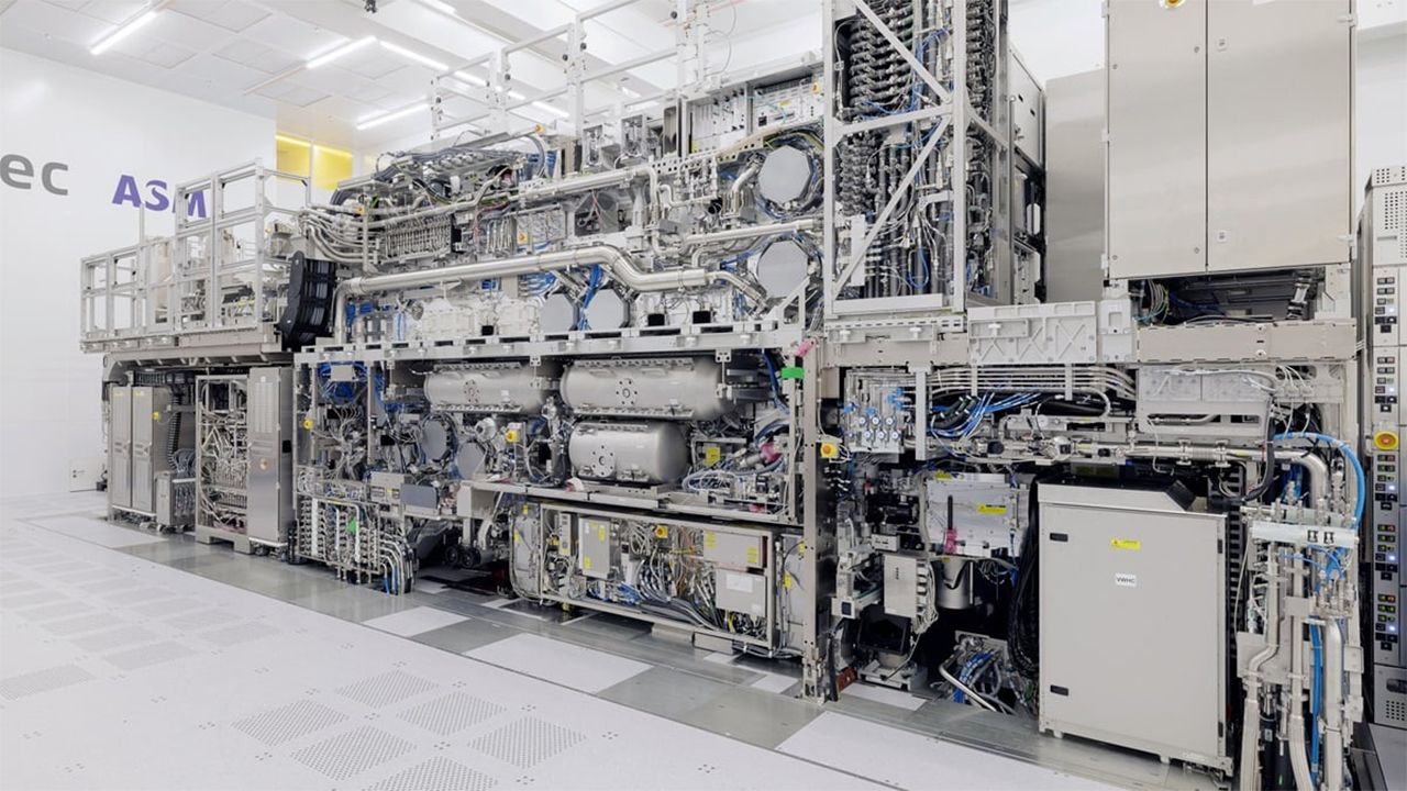
To understand why this transition is both critical and challenging, it is helpful to examine the fundamental physics of the equipment involved. High-NA EUV lithography tools are capable of achieving a single-exposure resolution of approximately 8 nanometers, a significant improvement over the 13-nanometer single-exposure resolution provided by current Low-NA EUV systems. This enhanced resolution allows chip designers to print much finer circuit features without resorting to complex multi-patterning techniques that introduce cumulative errors and manufacturing delays. However, when these advanced High-NA scanners are operated with conventional six-by-six-inch photomasks, they suffer from a major geometric limitation: their exposure field is reduced to precisely half the area of their Low-NA counterparts.
This reduction in the exposure field creates profound engineering obstacles for companies attempting to manufacture very large silicon dies, such as the massive artificial intelligence accelerators and high-performance computing processors that dominate modern data centers. To work around this limitation using standard six-by-six-inch masks, chipmakers are currently forced to choose between stitching multiple exposure fields together on a single wafer or shifting entirely toward multi-chiplet architectural designs. Both of these fallback approaches introduce their own distinct sets of engineering compromises, including reduced tool productivity, increased manufacturing costs, and higher power consumption during operation. To circumvent these photomask limitations entirely, TSMC is actively collaborating with lithography pioneer ASML to lay the groundwork for a transition to six-by-12-inch photomasks.
Rewriting the standard size of photomasks used in global semiconductor manufacturing is by no means a trivial endeavor. It requires a comprehensive, industry-wide overhaul that touches virtually every aspect of the chip production ecosystem. Everything from electronic design automation (EDA) software tools to the specialized equipment used to produce and write the masks—as well as the robotic handling systems that transport them through cleanrooms—must be completely redesigned and re-engineered. Consequently, success depends on seamless cooperation across the entire semiconductor supply chain.
ASML has expressed considerable optimism regarding this monumental transition, bolstered by the fact that the initiative has garnered robust backing not only from TSMC, but from industry heavyweights Intel and Samsung as well. Christophe Fouquet, president and CEO of ASML, emphasized the collaborative nature and necessity of the shift in a recent statement to the industry.
"We expect the adoption of High NA EUV to increase progressively along the device scaling roadmap, first using current 6-inch masks and then further supported by 12-inch masks, which enable greater scanner productivity and allow the industry to meet the demand for smaller, faster and more energy-efficient chips," said Fouquet. "We are pleased by the strong initial support of semiconductor manufacturers, mask suppliers and partners for this initiative."
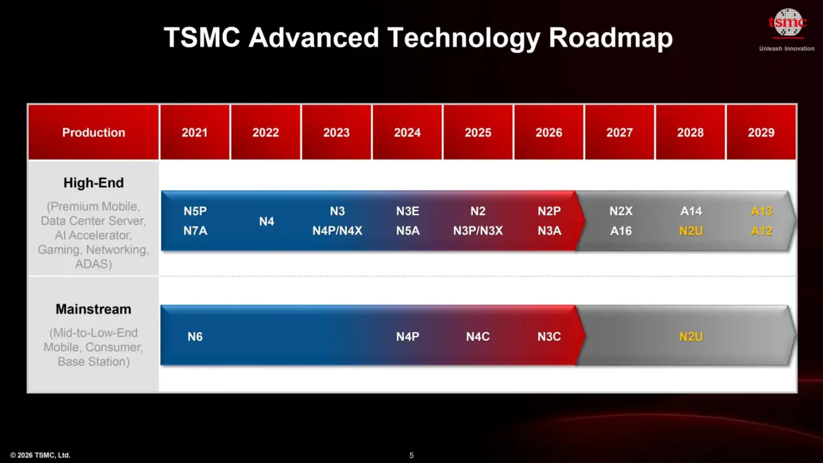
Despite these broad industry alignments, perhaps the most compelling intrigue surrounding TSMC’s adoption strategy is precisely which process technology node will earn the milestone of being the first to utilize the new High-NA systems. Reviewing TSMC’s recently unveiled process technology roadmap provides significant context for speculation. The company’s current strategy is divided into two distinct tracks: annual, client-oriented process nodes such as N2, N2P, N2X, A14, and A13, alongside roughly biennial high-performance nodes, which include A16 scheduled for 2027, followed by A12 in 2029. TSMC has already explicitly confirmed that its upcoming A12 and A13 nodes, both slated for rollout in 2029, will continue to rely exclusively on conventional Low-NA EUV lithography technology.
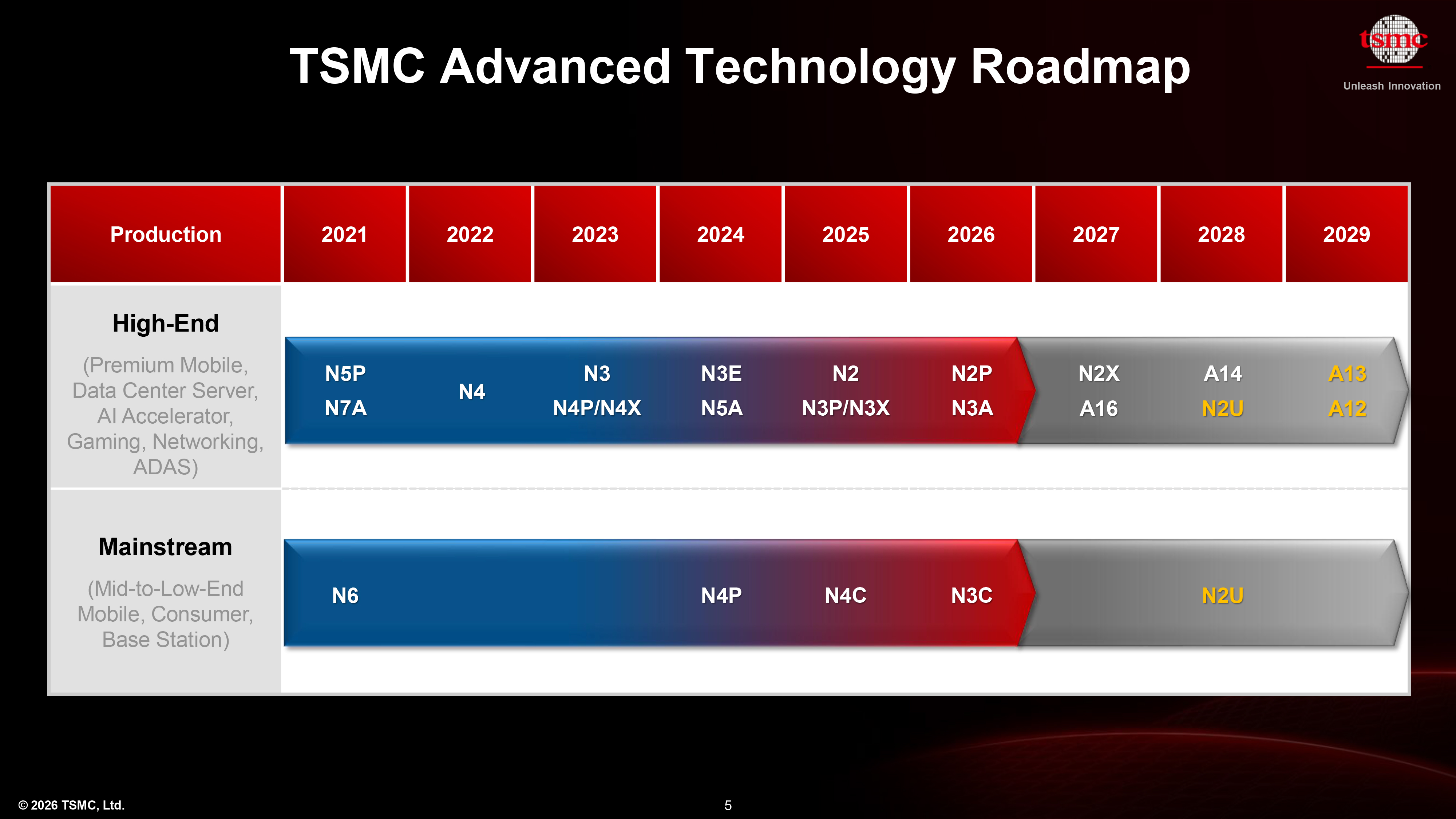
Because the A13 node is essentially structured as an optical shrink of the preceding A14 technology—yielding a modest transistor density increase of just 6 percent, with specific performance and power metrics yet to be formally detailed—its successor arriving in 2030 will face immense pressure to deliver substantially larger gains. It is therefore entirely logical to anticipate that the successor to A13, whether it ultimately receives the commercial designation of A11 or A10, will transition to more advanced lithography equipment, potentially incorporating TSMC’s third-generation nanosheet gate-all-around transistors. Such a combination would be necessary to achieve significantly higher transistor density alongside meaningful improvements in power efficiency and raw performance compared to preceding generations, though industry analysts acknowledge that these specific node assignments remain subject to change as development milestones draw closer.

Leave a Reply