
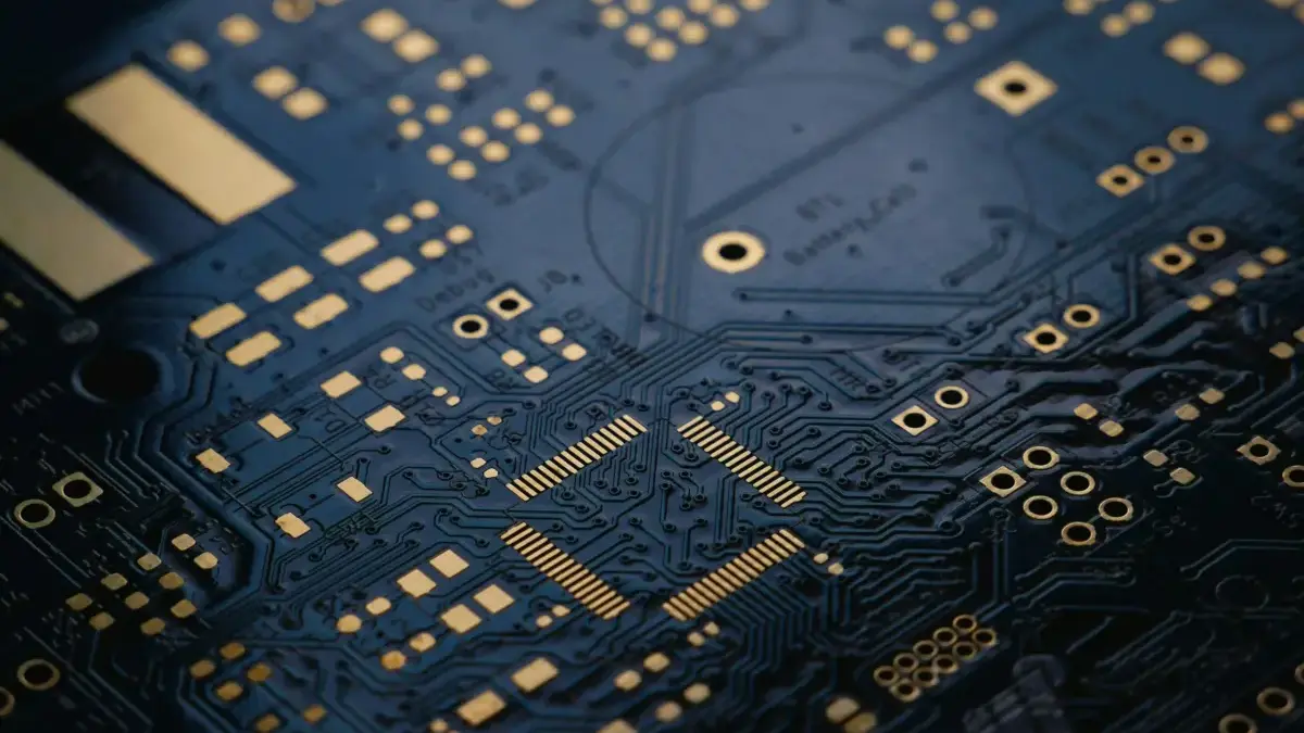
The electronics engineering landscape is undergoing a profound structural shift as the industry moves away from entirely human-driven layouts toward sophisticated, algorithm-assisted design. This evolution is reshaping how engineers approach printed circuit board (PCB) design and prototype services, fundamentally altering the timelines and methodologies of hardware development.
For decades, the physical layout phase of a circuit board has been a notorious bottleneck, requiring weeks of painstaking manual routing, component placement, and design rule checking. Today, advanced artificial intelligence and machine learning tools are capable of analyzing thousands of potential configurations in a matter of minutes. By doing so, these platforms help engineering teams identify potential electrical, thermal, and manufacturing issues much earlier in the prototyping phase.
For electronics development teams currently evaluating custom PCB prototyping options, these emerging AI-assisted workflows highlight several key performance advantages. Chief among them are significantly faster design iteration cycles, stronger routing discipline enforced by algorithms, and tighter, more reliable handoffs from the engineering desk to the manufacturing floor. As hardware systems grow increasingly complex, incorporating AI into Electronic Design Automation (EDA) is no longer viewed as a futuristic concept, but as a practical necessity for staying competitive.
Redefining Design Cycles with AI Automation
At its core, circuit board design requires human professionals to make thousands of individual, highly consequential decisions regarding component positioning, intricate trace routing, and multi-layer allocation. In traditional workflows, these repetitive and computationally heavy tasks could consume days or even weeks of senior engineering talent. Automated and physics-driven AI tools are now compressing those schedules dramatically, while simultaneously assisting engineers in evaluating comprehensive design integrity and electrical performance right from the earliest stages of development.
Recent real-world benchmarks underscore the magnitude of this transformation. Quilter, a developer of physics-driven AI tools for hardware design, recently demonstrated the capabilities of its platform through an intensive project involving a functioning two-board computer system. In that undertaking, a single engineer utilized Quilter’s platform to complete the design in under a week.
The entire project required just 38.5 hours of human input, a stark contrast to traditional industry estimates of 428 hours for the same scope of work. Breaking down the metrics, the company reported that the baseboard alone required just 12 hours of work against a conventional manual quote of 238 hours, while the more specialized system-on-module required 26.5 hours instead of an estimated 190 hours.

Efficiency gains of this scale carry profound implications for corporate research and development budgets. Organizations are now empowered to test multiple design approaches, stackups, and architectural concepts before committing to expensive physical production runs. Identifying architectural flaws or routing bottlenecks early in the simulation phase drastically reduces the risk of expensive respins after manufacturing. Consequently, highly skilled engineering resources can be redirected away from tedious manual placement and routing chores and toward solving novel, high-level technical challenges.
Optimizing the Custom PCB Prototype
The modern prototyping phase relies heavily on platforms that can ingest vast patterns from historical projects and present engineers with optimized design options. These algorithms draw upon extensive repositories of design data accumulated from thousands of successfully completed boards. By analyzing this historical data, machine learning models can identify successful layout strategies without requiring explicit, manual programming for every unique project scenario.
Industry observers and manufacturing partners have noted this transition. According to insights shared by EMSG, AI-powered design assistants can effectively suggest optimal component placements, routing paths, and layer configurations. Engineers tasked with developing a custom PCB prototype can leverage these platforms, which utilize historical data and machine learning to generate recommendations rooted in approaches that have historically performed well in previous, comparable designs.
Significantly, this technology is not intended to replace human expertise, but rather to augment it. The platforms provide informed, data-backed suggestions that professional hardware engineers can accept, modify, or reject based on specific project requirements, form-factor constraints, and architectural limitations.
Real-time assistance during active development helps designers explore creative solutions while maintaining strict technical rigor. Automated analysis handles repetitive evaluation tasks, leaving professionals free to focus on innovation and strategic decision-making. Ultimately, the technology accelerates development cycles while firmly keeping final engineering decisions, validation, and sign-offs in the hands of the design team.
Accelerating Component Placement
Positioning hundreds or even thousands of individual components represents one of the most computationally intensive challenges in modern board development. Component placement directly dictates subsequent signal integrity, thermal management performance, and overall manufacturing feasibility.

Conventional design approaches have long relied on experience-based heuristics. While these rules-of-thumb work reasonably well for simple layouts, they consistently struggle when applied to dense, modern designs containing multiple functional blocks, mixed-signal domains, and strict electrical requirements. AI algorithms address these limitations by evaluating vast solution spaces against a multitude of complex constraints simultaneously. This allows engineers to explore layout options that would be virtually impossible to assess manually within the same timeframe.
Cadence Design Systems has demonstrated the practical, commercial impact of this capability through its Allegro X AI technology. According to Saugat Sen, VP of product marketing at Cadence, one undisclosed customer was grappling with a complex design that traditionally took three days to complete using manual human placement methods. When processed through the AI-enabled platform, the placement time dropped to just 75 minutes. Beyond the dramatic reduction in processing time for complex boards, the platform also achieved a 14% improvement in total wire length.
Shorter electrical connections inherently support better signal integrity, lower propagation delay, and can reduce overall routing complexity and manufacturing costs. However, the exact downstream effects on electromagnetic interference (EMI) and production costs remain closely tied to the board’s specific stackup, materials, power delivery requirements, and chosen manufacturing processes.
With these tools, hardware professionals can now conduct thorough early-phase feasibility analyses by rapidly testing multiple layout configurations. Rather than blindly committing to a single approach based on limited initial assumptions, engineering teams can compare several distinct layout configurations before investing significant time in detailed routing work.
Solving Complex Routing and Manufacturing Challenges
Modern high-performance circuit boards often function much like complex metropolitan areas equipped with multilevel road systems, where hundreds of connection points require meticulous planning. Bridging upper and lower conductive layers requires vias—plated holes that create electrical connections between layers so signals and power can traverse the board stack. However, every via introduced into a design inherently adds unwanted electrical parasitics and interference, while simultaneously increasing manufacturing complexity and fabrication cost. This dynamic creates a severe optimization challenge for designers working with dense, high-performance layouts.
InstaDeep has approached this persistent industry problem through its DeepPCB platform, which deploys specialized algorithms to evaluate and refine complex routing options. When tested on a demanding benchmark board containing 444 airwires and 157 nets, the company reported that the system has demonstrated substantial, measurable improvements over successive development cycles.

According to DeepPCB, the platform achieved a remarkable reduction of over 50% in via count over the past year. By identifying clean, efficient routing paths that conventional planning methods might easily overlook during standard manual layout sessions, the software produces significantly optimized board configurations.
Reducing unnecessary vias simplifies the physical fabrication process and frequently improves critical electrical characteristics. Nevertheless, overall manufacturing yield and long-term reliability depend heavily on the holistic board design, meticulous material selection, strict fabrication tolerances, and the thoroughness of the inspection process.
As modern circuit boards contain fewer potential physical points of failure, manufacturing yields improve organically, while streamlined layouts accelerate overall production timelines. By applying lessons learned from previous completed projects, the technology helps engineering teams refine their strategies to tackle increasingly complex routing scenarios with greater consistency and lower failure rates.
The Future of Hardware Engineering
The integration of automated routing and placement tools is successfully dismantling bottlenecks that have historically constrained hardware development timelines. By delegating repetitive layout tasks to intelligent algorithms, organizations are finding new room to focus on core innovation and rigorous testing. Organizations developing a custom PCB prototype can now allocate substantially more resources toward perfecting product functionality before ever committing to expensive production tooling.
Despite these advances, industry consensus suggests that AI-assisted placement and routing are unlikely to eliminate the need for experienced, highly skilled PCB designers. The more immediate and profound value of these tools lies in their ability to dramatically reduce the time required to evaluate alternatives, allowing engineering teams to test a wider array of configurations before committing to fabrication. As the industry marches forward, the next critical challenge for hardware teams will be proving that these accelerated workflows consistently produce physical designs that meet demanding electrical, thermal, and manufacturing requirements in the real world.


Leave a Reply