
In the highly competitive landscape of modern electronics manufacturing, the pursuit of zero defects remains the ultimate operational objective. Within this demanding sector, even a single malfunctioning Printed Circuit Board Assembly (PCBA) can cascade into severe operational consequences, including expensive product recalls, severely damaged brand reputations, and significant safety hazards for end-users. To successfully safeguard against these risks and ensure the delivery of high-quality, reliable electronic products, manufacturing enterprises must deploy a robust, comprehensive validation strategy from the ground up.
However, designing and implementing such a strategy presents a distinct engineering challenge. Choosing the right testing methodology when options such as In-Circuit Testing, Functional Testing, Bed-of-Nails architectures, and Flying Probe systems are on the table can prove exceptionally complex to navigate. Industry leaders are increasingly realizing that these testing pillars should not be viewed in isolation. Instead, exploring how to integrate these diverse methodologies is the key to streamlining complex production lines, optimizing throughput, and securing long-term manufacturing excellence.
The Core Distinction: In-Circuit and Functional Testing
The historical debate surrounding In-Circuit Testing versus Functional Testing has often framed these two methodologies as competing approaches. In reality, industry experts and technical authorities understand that they are deeply complementary pillars of any successful quality assurance program.
In-Circuit Testing acts as the foundational auditor of the PCBA. By systematically probing individual components and their underlying interconnections, it confirms electrical continuity, detects accidental shorts or opens, and meticulously validates crucial component values such as resistance and capacitance. The primary focus of ICT is to identify manufacturing defects early in the production cycle—such as soldering errors, component misplacement, or out-of-tolerance parts—effectively answering the fundamental question of how well the board was physically built.

Functional Testing, on the other hand, takes a much more holistic view of the assembly. It evaluates the integrated performance of the entire PCBA under simulated real-world operating conditions, assessing dynamic parameters such as voltage regulation, current draw, power factor, and operational cycles. By answering the critical question of whether the device works as intended, FCT successfully identifies latent design flaws and complex system-level integration bottlenecks that component-level audits might miss.
In high-volume, large-scale production environments, standard protocol dictates that ICT should always be executed before FCT. Utilizing In-Circuit Testing as an initial, rigorous quality gate to filter out assembly defects prevents manufacturers from wasting valuable time, labor, and resources on boards that are structurally doomed to fail the more expensive and time-consuming Functional Test later in the workflow.
Choosing the Right Automatic Tester: Bed-of-Nails Versus Flying Probe
Once engineering teams determine what needs to be tested, they must immediately address how the testing will be physically executed. This equipment choice typically boils down to two dominant automated test equipment technologies: Bed-of-Nails systems and Flying Probe systems, each offering distinct advantages depending on production scale and board complexity.
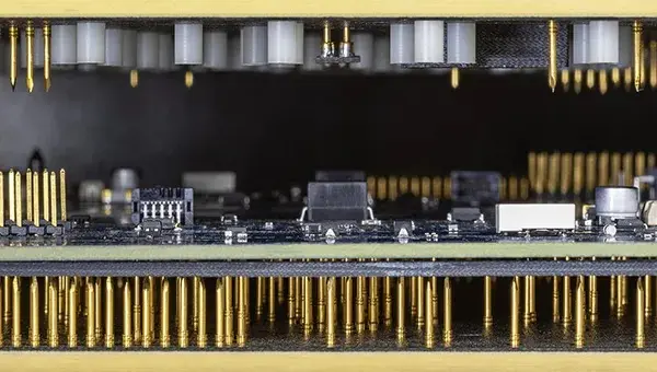
Bed-of-Nails testers utilize a fixed, custom-engineered matrix of spring-loaded pins that make simultaneous contact with specific, pre-determined test points across the PCBA. Because the hardware fixture is custom-made for a specific board layout, this method allows for the simultaneous testing of multiple points, delivering exceptional speed and high throughput. This performance profile makes Bed-of-Nails testers the superior choice for high-volume, mature product lines where the initial financial investment in a custom test fixture is quickly offset by significant long-term operational efficiency.
In stark contrast, Flying Probe testers operate without custom mechanical fixtures. Instead, they utilize highly agile, movable probes that physically fly to designated test points across the board’s surface under computer control. Because no dedicated fixtures are required, this methodology significantly lowers initial setup costs and allows manufacturers to adapt rapidly to frequent design changes, engineering revisions, or low-volume prototype runs. This technology proves particularly invaluable for complex, dense boards where traditional test pads are limited, restricted, or entirely inaccessible to fixed mechanical pins.

However, selecting the correct test equipment must account for several fundamental pillars of modern PCBA testing requirements. Test point placement and mechanical access dictate whether an ICT tester can physically and electrically reach every single node it is meant to verify. This is a critical Design for Testability decision made months before a physical board ever reaches the assembly and test floor, ultimately determining which equipment architecture is even viable. Bed-of-Nails testers require dedicated, fixed-position test pads laid out precisely during the initial design phase, whereas Flying Probe systems can easily reach arbitrary points on the substrate and tolerate much less generous test point provisioning.
As the global push toward electronic miniaturization continues unabated, dedicated test pads are rapidly disappearing from modern board layouts. Traditional Bed-of-Nails testers, which rely heavily on a rigid, fixed pin matrix, frequently prove structurally inadequate for these ultra-dense designs. When high-density layouts render traditional test pads inaccessible, Flying Probe testers become an absolute operational necessity. Because they eliminate the need for physical custom fixtures, they provide the necessary agility to probe arbitrary points on a crowded board without compromising test coverage.
Furthermore, the physical interface established between testing hardware and the delicate PCBA represents one of the most sensitive points of the entire manufacturing process. Inadequately modulated contact force can result in irreversible mechanical damage, such as microscopic surface abrasions that trigger latent field failures, or alternatively, frustrating false negatives caused by poor electrical connectivity. Modern, high-reliability manufacturing demands extreme precision in landing force control. Advanced Automated Test Equipment platforms incorporate high-speed linear motors designed to provide a soft-touch interaction with the substrate. These sophisticated systems employ predictive software algorithms to accurately map the board layout, preventing damaging probe collisions and ensuring that the structural integrity of delicate substrates remains completely uncompromised throughout the diagnostic cycle.
Beyond basic electrical continuity checks, standard testing methodologies often fail to identify insidious faults—such as signal integrity degradation or subtle parametric drift—that might successfully pass initial inspection today but cause catastrophic field failures tomorrow. To consistently reach zero-defect manufacturing targets, hardware architectures must support a multi-domain diagnostic approach. This advanced strategy involves integrating Parametric ICT with artificial intelligence-driven data analysis. By evaluating whether a component is trending toward failure—where a part remains technically within specification today but drifts toward operational collapse in the near future—and utilizing dynamic defect databases to automate diagnostics, manufacturers can successfully shift their operational posture from reactive troubleshooting to true predictive reliability engineering.
The Synergistic Approach: Integrating Test Methodologies
Industry veterans recognize that the most efficient PCBA validation strategy is rarely about choosing just one exclusive method; rather, it centers on leveraging the respective strengths of multiple technologies in tandem. In highly demanding sectors such as automotive manufacturing, aerospace engineering, and defense systems, where operational reliability is absolute and non-negotiable, industry leaders are increasingly adopting deeply integrated workflows and hybrid test stations.

The true power of this integrated strategy lies in synergy. By thoughtfully combining In-Circuit Testing and Functional Testing, manufacturers secure comprehensive fault coverage, successfully capturing granular assembly faults and system-level design flaws within a streamlined processing window. Moreover, there is profound strategic value in orchestrating both Bed-of-Nails and Flying Probe technologies within the same broader manufacturing test cycle. These systems are capable of working in concert to optimize the overall testing workload efficiently across diverse product lines.
For instance, a Flying Probe test station serves as an ideal environment for checking delicate components that remain inaccessible to a rigid Bed-of-Nails fixture, performing initial optical inspections, or executing net tests on early-stage prototypes. Once those specific, intricate validations are successfully completed, the mature PCBA can smoothly transition to a Bed-of-Nails station designed specifically for high-throughput power-on testing, firmware flashing, and rapid functional validation. This collaborative, multi-tiered approach maximizes overall test efficiency, guarantees comprehensive fault coverage, and allows producers to capitalize on the distinct advantages of both systems—pairing the unmatched flexibility of Flying Probe technology with the high-volume processing speed of Bed-of-Nails architecture—without sacrificing manufacturing throughput.
Achieving excellence in modern PCBA manufacturing requires a clear-eyed understanding of the distinct, complementary roles played by In-Circuit Testing and Functional Testing. By intelligently integrating Bed-of-Nails systems for high-volume operational stability and Flying Probe technology for agile flexibility, production lines can be thoroughly optimized for both uncompromised quality and rapid speed-to-market.
Implementing an effective testing strategy demands a thorough, continuous analysis of production volumes and broader product lifecycles. By carefully aligning throughput requirements with integrated testing workflows, manufacturers can establish proactive quality gates that ensure assembly-related defects are thoroughly mitigated long before final product validation occurs. Enterprises currently facing operational bottlenecks within their existing testing workflows are encouraged to reach out to engineering specialists for tailored consultations regarding their overarching PCBA testing strategies.



Leave a Reply