
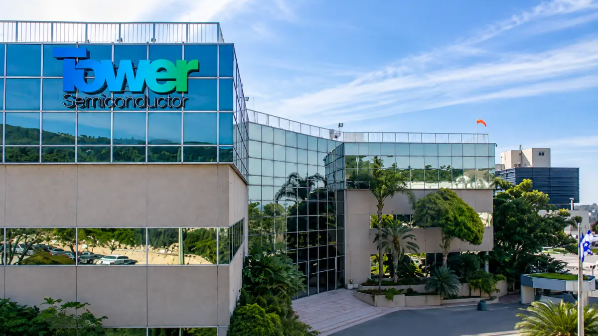
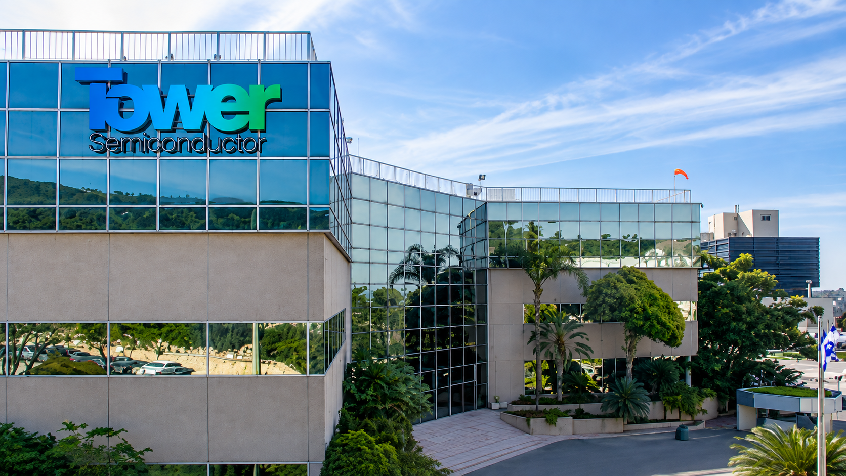
Tower Semiconductor and the government of Japan are moving forward with a massive co-investment plan totaling $4 billion to transform the specialty foundry’s regional fabrication facilities into a primary global manufacturing base for optical-connectivity semiconductors. According to reports from the industry, this ambitious capital expenditure initiative involves a comprehensive restructuring of Tower’s Japanese operations. The strategy relies on a dual-track expansion model designed to repurpose an idled fab, maximize the production output of an existing 300mm facility, and eventually integrate an additional 300mm wafer fab into the network. Through these coordinated efforts, the company aims to scale its Japanese production capacity dramatically, targeting the equivalent of 45,000 300mm wafers per month by the year 2029.
The global semiconductor landscape has shifted dramatically over recent years, with governments and major foundries alike placing a heightened emphasis on regional supply chain resilience, advanced packaging capabilities, and specialized manufacturing nodes. While much of the mainstream semiconductor discourse tends to focus on leading-edge logic chips for smartphones and artificial intelligence accelerators, the backbone of modern digital infrastructure relies heavily on specialized analog, mixed-signal, and optical semiconductors. These components are vital for managing data transmission speeds, power efficiency, and signal integrity across massive data centers and telecommunications networks. By concentrating its optical semiconductor manufacturing efforts in Japan, Tower Semiconductor is positioning itself at the center of this burgeoning technological demand, backed by substantial financial and strategic support from the Japanese government.
Track One: Convert and Expand
The first phase of Tower Semiconductor’s comprehensive strategy centers on revitalizing existing infrastructure and accelerating output through a two-pronged approach of conversion and expansion. The primary objective of this track is to breathe new life into idle manufacturing assets while simultaneously pushing an operational 300mm facility to its absolute maximum efficiency. Converting an idled fabrication plant into a modern, highly specialized cleanroom environment allows the foundry to bypass the immense lead times and astronomical greenfield construction costs typically associated with building a semiconductor plant from the ground up. Instead, Tower can focus its capital on retrofitting the facility with state-of-the-art tools tailored specifically for the intricate processes required to manufacture advanced optical-connectivity chips.
At the same time, the company is pouring resources into its existing 300mm operations in Japan to extract higher volumes and tighter tolerances. Modern optical semiconductors require precise manufacturing controls, specialized substrates, and advanced photonics integration techniques that differ significantly from standard silicon processing. By optimizing the workflow, upgrading lithography and etching tools, and streamlining material handling within the current 300mm footprint, Tower can immediately begin scaling its output to meet near-term market demands. This immediate capacity increase serves as a crucial bridge while the heavier lifting of long-term facility conversions and subsequent expansions takes place over the remainder of the decade.
The broader implications of this dual-track strategy extend well beyond Tower Semiconductor’s corporate balance sheet. Japan has been aggressively working to rebuild its domestic semiconductor manufacturing prowess, partnering with international foundries and technology leaders to secure a stable supply of crucial components for its industrial base. The collaboration with Tower aligns neatly with Japan’s broader industrial policy goals, which seek to attract foreign investment, foster high-tech engineering talent within the region, and secure a prominent role in the next generation of digital infrastructure. As data centers expand globally to support cloud computing, enterprise artificial intelligence workloads, and high-frequency telecommunications, the demand for optical transceivers and high-speed interconnects has skyrocketed. By establishing a dedicated, high-volume manufacturing hub in Japan, Tower is creating a specialized ecosystem capable of supplying these critical components on a massive scale.
As the project progresses toward its ultimate 2029 targets, the combination of the retrofitted facility, the maximized output of the existing 300mm plant, and the planned addition of a brand-new 300mm fab will culminate in a staggering forty-fold increase in regional output compared to legacy baselines. This massive scaling effort reflects both the long-term confidence in optical connectivity technologies and the strategic alignment between private foundry operations and government-backed industrial initiatives. With preparations underway and capital deployment moving forward, Tower Semiconductor’s Japanese operations are set to become a cornerstone of the global optical chip supply chain for the foreseeable future.



Leave a Reply