
Intel Foundry has successfully transitioned ASML’s advanced high numerical aperture (High-NA) extreme ultraviolet (EUV) lithography tools into active production, marking a critical milestone for next-generation semiconductor manufacturing. However, even as the hardware proves its viability in the fab, the industry continues to grapple with a more complex engineering barrier: stitching together larger chip designs across multiple exposures to achieve high-volume manufacturing without sacrificing yield.
The milestone was highlighted by Intel’s disclosure that High-NA EUV has now been utilized on more than one million wafers spanning tool certification, research and development, and live production environments. This includes select layers incorporated into a subset of upcoming Intel Core Ultra Series 3 processors, carrying the code name Panther Lake. According to the company, key operational metrics such as overlay accuracy, throughput, and tool availability are meeting expectations. Furthermore, the High-NA-patterned layers on the Intel 18A process node have delivered yield, defect density, electrical performance, and reliability that are directly comparable to layers processed using conventional 0.33-NA EUV equipment.
Despite these encouraging achievements, the successful production of Panther Lake does not signal that the semiconductor industry has fully solved the intricate challenges of die stitching. The layers patterned with High-NA technology for Panther Lake were carefully and deliberately chosen so that no critical electrical connections needed to cross the boundary line between the two half-fields. The primary objective of this initial deployment was to demonstrate that High-NA tools could operate reliably inside a real-world production flow and to gather essential manufacturing experience without introducing performance risks to the finished consumer product.
This distinction is vital because the fundamental physics and optics of High-NA systems introduce an inherent field-size limitation.

Why High-NA Needs Stitching
Traditional 0.33-numerical aperture EUV systems can expose a full reticle field measuring 26 mm by 33 mm using a standard 6-inch by 6-inch photomask. By increasing the numerical aperture to 0.55, High-NA technology significantly improves optical resolution and allows for finer feature scaling. However, to achieve this optical enhancement, its anamorphic optics cut the exposure field size precisely in half, reducing the usable area to 26 mm by 16.5 mm.
For chip designs that can fit entirely within that constrained half-field, the transition poses no complications. But for larger, high-performance processors, graphics chips, and artificial intelligence accelerators, the smaller field presents a major roadblock. Larger designs require either two separate exposures that are carefully stitched together during the manufacturing process or, eventually, the adoption of a larger mask format.
As advanced semiconductors continue to grow in physical size to accommodate more transistors and compute engines, the necessity for reliable stitching has intensified. Chris Mack, co-founder and CTO of Fractilia, a lithography metrology software company, noted in an interview that the industry’s reliance on large-scale silicon is driving the demand for full-field High-NA patterning. Because modern AI accelerators and enterprise processors frequently push the boundaries of conventional reticle fields, finding a robust method to manage boundaries is critical.
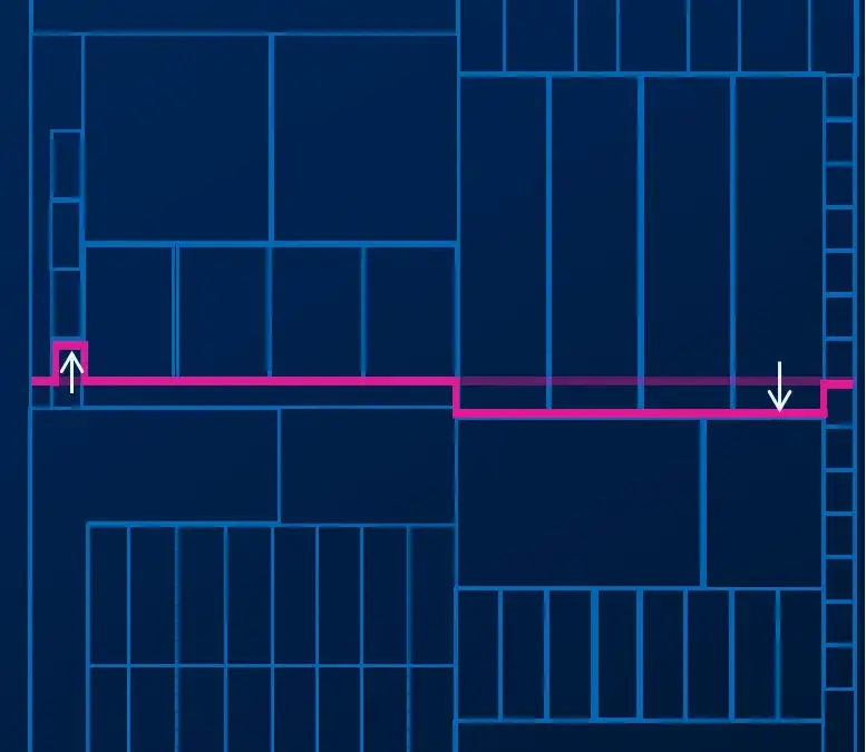
Intel Foundry is actively exploring multiple methodologies to make multi-exposure stitching feasible at scale. The most straightforward approach—and the one utilized for Panther Lake—is to design the chip layout so that no electrically significant signal paths cross the seam between exposures. A slightly more flexible strategy is known as block-and-route stitching. In this method, chip architects carefully position the boundary so that critical standard-cell circuitry is kept entirely on one side, allowing routing connections to travel safely through higher metal layers instead of breaking across the seam.

Mark Phillips, a distinguished engineer at Intel Foundry, described block-and-route as a foundational stepping stone within a broader strategy designed to maximize the utility of standard 6-inch masks on High-NA equipment. Beyond basic block-and-route techniques, Intel is developing a more advanced methodology referred to as two-dimensional, or "Zipzag," stitching. In this configuration, the physical seam between exposures does not follow a rigid straight line across the die.
The name draws inspiration from the common zigzag stitch used in textiles. Rather than forcing the boundary between the two High-NA exposures to cut straight across sensitive active areas, Zipzag allows the boundary line to jog around critical regions of the microarchitecture. This grants chip designers significantly more freedom to keep vulnerable circuitry safely away from the stitching interface, though it concurrently introduces substantial complexity into mask construction, optical inspection, and overall fab process control.
Electrical Proof Comes in Stages
Intel has already completed electrical verification of the block-and-route technique using a full-loop test chip featuring a straight-line seam. The evaluation involved test structures designed to compare the electrical resistance and variation of metal lines crossing the stitching boundary directly against control structures that avoid the seam entirely. Additional chain and comb structures were deployed across the wafer to screen effectively for unintended electrical shorts and opens.
The latest iterations of Zipzag test chips take these evaluations a step further by incorporating electrical test structures that span a jogged seam. Inline physical imaging, overlay measurements, and defect scans indicate that the jogged boundary regions are structurally sound, though final electrical test results are still pending comprehensive analysis.

Industry experts view block-and-route as a manageable near-term hurdle. Chris Mack observed that the technique appears relatively straightforward and carries low risk, making it the most logical path for semiconductor manufacturers embarking on their first multi-exposure stitching exercises.
Feature stitching, however, represents a far more formidable challenge. This occurs when critical device features themselves must cross the boundary line between two distinct exposures, demanding exceptionally tight operational control over how the separate optical patterns overlap. Scaling such a technique for high-volume manufacturing requires managing far more than simple overlay precision. Parameters such as exposure dose, focal plane stability, edge placement error, and stochastic variations all become critical variables.
The Seam Must Survive Statistical Tails
Mack emphasized that the stitching errors of primary concern to process engineers can measure only a few nanometers, a scale comparable to inherent stochastic edge roughness on the wafer. Because of this tight tolerance margin, semiconductor fabricators must successfully isolate and distinguish systematic errors introduced by the stitching process from the random variations that naturally occur during extreme ultraviolet lithography.
This analytical challenge is further complicated by the limitations of metrology tools. Scanning electron microscopes, which serve as the industry workhorse for measuring microscopic feature dimensions, inherently introduce image noise that can easily mimic real stochastic variation on the silicon. To overcome this hurdle, Fractilia has been collaborating closely with Intel on advanced mathematical and algorithmic methods designed to separate measurement noise from actual systematic stitching discrepancies.

Furthermore, looking merely at average performance metrics is insufficient for high-volume semiconductor production. Mack pointed out that rare manufacturing failures residing in the long tails of statistical distributions can emerge at parts-per-million or even parts-per-billion frequencies. A stitching process that appears perfectly healthy on average can still generate severe yield degradation once millions of complex chips are pushed through high-volume manufacturing lines. Consequently, true production yield remains the ultimate unknown until extensive, multi-wafer experiments are completed.
This underlying uncertainty directly impacts the economic calculus between deploying High-NA lithography versus sticking with multi-patterning approaches using older 0.33-NA EUV tools. While process engineers can model the direct financial cost of performing one High-NA exposure against two, three, or four lower-NA exposures, the economic equation shifts dramatically depending on which method ultimately yields better working silicon.
Intel’s Panther Lake experiment was never intended to prove an immediate economic advantage over multi-patterning. Instead, the High-NA process layer was introduced as a direct replacement for an established 0.33-NA step in a manner specifically intended to leave the functional characteristics of the finished processor unchanged. The exercise served primarily as a production readiness assessment to understand how ASML’s advanced optical tools behave under demanding manufacturing schedules.
Larger Masks Could Remove the Seam
Over the long term, die stitching may become entirely unnecessary as the lithography ecosystem evolves. Intel and ASML are actively encouraging the broader semiconductor supply chain to transition toward larger 6-inch by 12-inch photomasks. A mask with double the physical length in one dimension would allow a High-NA scanner to expose a full conventional reticle field in a single shot, completely eliminating the need for multi-exposure stitching. Furthermore, Intel notes that the larger format could enhance operational productivity on existing 0.33-NA EUV equipment by combining tasks that currently require two separate 6-inch masks.

While Mack believes that multi-exposure stitching will successfully support initial product generations, he views the adoption of larger masks as the ultimate, preferred solution for the industry. The productivity gains derived purely from utilizing a 6-inch by 12-inch mask infrastructure will ultimately justify the industry-wide transition.
However, that transition will not occur overnight. Based on technical discussions held at the SPIE Photomask Technology + Extreme Ultraviolet Lithography conference in Monterey, industry stakeholders estimate that it will take roughly five years to achieve initial mask demonstrations, and up to seven years before such large masks can be routinely deployed to print production wafers in high volumes.
That timeline ensures that die stitching will play a vital role in advanced semiconductor fabrication for years to come. Intel has conclusively demonstrated that High-NA lithography hardware can operate successfully inside an active high-volume fab environment. The immediate challenge ahead lies in making stitching sufficiently predictable, measurable, and design-friendly so that chipmakers can leverage the benefits of the smaller High-NA field without compromising overall production yield. The optical tools are securely installed on the fab floor, and the industry’s focus has now shifted to mastering the complex ecosystem required to support them.

Leave a Reply