
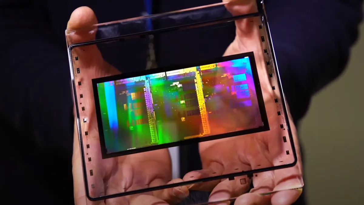
Intel announced on Wednesday that it has officially begun installing essential production tools at its state-of-the-art Fab 62 facility located in Arizona. This critical milestone keeps the advanced manufacturing site firmly on track to achieve full-scale mass production by late 2028. The development marks a major step forward in the company’s broader strategy to expand its domestic manufacturing footprint, secure supply chain resilience, and reinforce American leadership in semiconductor fabrication. Alongside the Arizona progress, the company also reported substantial advancements at its massive Ohio One manufacturing complex, signaling steady momentum across its multi-state expansion initiatives. Furthermore, Intel confirmed a monumental technical achievement: the successful integration of High-Numerical Aperture Extreme Ultraviolet (High-NA EUV) lithography into its high-volume manufacturing lines.
These operational milestones coincide with the company’s continued, heavy investments in domestic research and development for leading-edge process technologies, advanced packaging solutions, and specialized photomask production capabilities. By anchoring these vital links of the semiconductor ecosystem within the United States, Intel maintains that its comprehensive approach sets it apart from competitors in the global semiconductor landscape. The realization of these advanced facilities underscores a deliberate strategy to control the entire lifecycle of semiconductor innovation on American soil, spanning fundamental physics research all the way to high-volume commercial wafer production.
Highlighting the strategic importance of this vertically integrated approach, Naga Chandrasekaran, executive vice president and chief technology and operations officer for Intel Foundry, emphasized the unique value proposition of domestic innovation. In a recent statement detailing the company’s manufacturing philosophy, Chandrasekaran pointed out the profound distinction between domestic fabrication and true domestic creation.
"There is an important difference between technologies made in America and technologies that are truly American-made," wrote Naga Chandrasekaran, executive vice president and chief technology and operations officer, Intel Foundry. "The difference lies in the research and development process that transforms ideas into manufacturable technologies."
This philosophy serves as the guiding principle behind Intel’s ongoing capital investments and technological rollouts. The installation of tools at Fab 62 in Arizona represents the physical manifestation of this philosophy, converting years of intensive laboratory research into tangible industrial capability. As tool installation moves forward, cleanrooms are outfitted with highly sophisticated machinery required to print nanometer-scale features onto silicon wafers, a meticulous process that demands absolute precision, vibration control, and ultra-clean environments. Fab 62 is designed from the ground up to support Intel’s most advanced process nodes, ensuring that when mass production commences in late 2028, the facility will be capable of churning out some of the world’s most powerful and energy-efficient processors.
While Arizona sees the beginning of tool hookups in Fab 62, Intel’s sprawling Ohio One complex is simultaneously taking shape. The Ohio project represents one of the largest single economic investments in the state’s history and is destined to become a cornerstone of America’s midwestern manufacturing corridor. Progress at Ohio One continues to advance steadily, with massive construction phases paving the way for eventual equipment move-ins. Together, the Arizona and Ohio developments form the twin pillars of Intel’s domestic foundry expansion strategy, designed to meet the surging global demand for cutting-edge compute power driven by artificial intelligence, cloud computing, and advanced client devices.
Crucial to achieving the performance metrics required for next-generation silicon is Intel’s successful integration of High-NA EUV lithography into its high-volume manufacturing environment. High-NA EUV systems represent the absolute cutting edge of semiconductor manufacturing equipment. By utilizing a higher numerical aperture, these advanced optical systems project light with a sharper resolution, allowing engineers to print increasingly smaller and denser features onto silicon wafers without resorting to complex multi-patterning techniques. Successfully transitioning High-NA EUV from the research lab into active, high-volume production lines is a monumental engineering feat that positions Intel at the forefront of lithographic capability. This technology is indispensable for scaling process nodes down to the most advanced nanometer dimensions, enabling greater transistor density, improved power efficiency, and higher performance for future computing architectures.
Beyond lithography and fab construction, Intel’s strategic advantage is heavily reinforced by its sustained commitment to end-to-end U.S.-based capabilities. The company continues to pour resources into leading-edge process technology R&D, ensuring a continuous pipeline of future nodes that follow current generations. Moreover, advanced packaging technologies—which allow multiple chiplets to be integrated seamlessly into a single package to boost performance and yield—are receiving significant investment and development within the United States. Photomask production, another critical step in translating circuit designs onto physical quartz templates used in lithography, is similarly maintained and cultivated domestically. By keeping these interdependent disciplines tightly coupled and geographically concentrated within the U.S., Intel fosters a collaborative feedback loop between research scientists, process engineers, and manufacturing operators.
This holistic ecosystem approach ensures that innovations conceived in the laboratory can be rapidly prototyped, refined, and scaled to high-volume manufacturing without the friction inherent in fragmented, internationally outsourced supply chains. As Fab 62 in Arizona advances toward its 2028 mass production target, and as work at Ohio One and other domestic sites progresses, Intel’s overarching vision of securing the future of advanced microelectronics manufacturing in the United States continues to materialize step by step.


Leave a Reply