
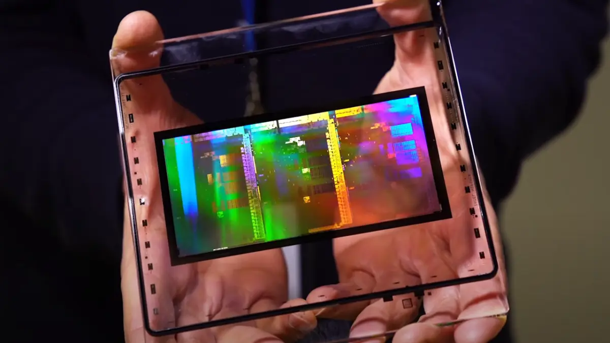
Intel announced on Wednesday that it has officially begun the critical process of installing production tools at its state-of-the-art Fab 62 facility in Arizona, marking a major milestone in the company’s ongoing efforts to scale domestic semiconductor manufacturing. According to the company’s timeline, the sprawling manufacturing site remains fully on track to achieve mass production by the late 2028 timeframe.
The announcement highlights a significant phase in Intel’s broader strategy to modernize and expand its American operational footprint. In addition to the progress in Arizona, the company reported steady and continued advancement on the construction and development of its massive Ohio One manufacturing complex. These facility updates coincide with a major technological milestone for the company: Intel confirmed that it has successfully integrated advanced High-Numerical Aperture Extreme Ultraviolet (High-NA EUV) lithography into its high-volume manufacturing workflows, positioning the firm at the cutting edge of semiconductor fabrication technology.
At the same time, Intel continues to pour substantial investments into its domestic research and development infrastructure, focusing heavily on leading-edge process technology, advanced packaging methodologies, and sophisticated photomask production capabilities within the United States. Company leadership emphasizes that this comprehensive approach—anchored by domestic research coupled with domestic manufacturing—provides a distinct competitive edge in the global semiconductor landscape.
"There is an important difference between technologies made in America and technologies that are truly American-made," wrote Naga Chandrasekaran, executive vice president and chief technology and operations officer for Intel Foundry, in a statement detailing the company’s strategic vision. "The difference lies in the research and development process that transforms ideas into manufacturable technologies."
The distinction highlighted by Chandrasekaran strikes at the heart of Intel Foundry’s value proposition as the company attempts to capture a larger share of the outsourced chip-manufacturing market. While several global competitors rely heavily on overseas research ecosystems or split their development and fabrication pipelines across disparate geographical regions, Intel’s model seeks to keep the entire lifecycle—from the initial conceptualization in research laboratories to advanced packaging and final high-volume production—closely aligned within domestic borders.
The installation of manufacturing tools at Fab 62 represents the physical realization of this vision in the American Southwest. Tool-in milestones are among the most closely watched events in the semiconductor industry. They signify that a cleanroom environment has reached the necessary standards of particulate control, structural stability, and utility hookups to begin receiving the multi-million-dollar lithography, etching, deposition, and inspection machinery required to build modern microprocessors.
Once these complex instruments are calibrated and brought online, they undergo rigorous qualification phases before transitioning to full-scale commercial output. By setting a target of late 2028 for mass production at Fab 62, Intel is providing visibility into its long-term capacity roadmap, ensuring that fabless designers and enterprise customers can plan their future hardware generations around guaranteed domestic supply lines.
Simultaneously, the progress reported at the Ohio One manufacturing complex underscores the sheer scale of Intel’s multi-site expansion strategy. The Ohio project, which represents one of the largest single private sector investments in the history of the state, is designed to create a massive manufacturing hub capable of supporting future nodes and meeting surging demand for advanced computational hardware. As structural work and infrastructure development continue at the site, Ohio One is slated to become a cornerstone of Intel’s future manufacturing network alongside its established operations in Oregon, Arizona, and New Mexico.
A critical enabler of Intel’s progress on these leading-edge nodes is the successful integration of High-NA EUV lithography into high-volume manufacturing. High-NA EUV systems represent the next generation of chipmaking equipment, featuring an optical design with a higher numerical aperture that allows for sharper light projection onto silicon wafers. This technological leap is essential for printing significantly smaller and denser transistor features without resorting to complex multi-patterning techniques, which can introduce delays and yield challenges. By successfully moving High-NA EUV from the research lab into active high-volume manufacturing lines, Intel is demonstrating its ability to absorb and deploy the world’s most advanced semiconductor machinery ahead of widespread industry adoption.
Beyond raw fabrication, Intel’s ongoing investments in advanced packaging and photomask production capabilities address other critical bottlenecks in the modern semiconductor supply chain. As traditional scaling approaches face physical limitations, the industry has increasingly turned to advanced packaging techniques—such as 2D and 3D chiplet integration—to combine multiple silicon dies into a single cohesive processor with improved performance and energy efficiency. By developing these packaging capabilities domestically, Intel ensures that American-made chips can be assembled and finished without relying on overseas third-party packaging houses. Similarly, maintaining cutting-edge photomask production in the U.S. secures the foundational blueprints used to pattern silicon wafers, safeguarding the intellectual property and manufacturing integrity of every chip produced.
Through this combination of tool installations at Fab 62, steady advancement in Ohio, the successful deployment of High-NA EUV lithography, and deep investments in R&D and advanced packaging, Intel is attempting to reshape the future of domestic technology manufacturing. As these projects move closer to commercial reality, the company maintains that its integrated approach to American innovation will continue to set it apart from industry competitors.

Leave a Reply