
GlobalFoundries has officially unveiled FDX Fusion at its facility in Dresden, introducing a brand-new generation of its fully depleted silicon-on-insulator (FD-SOI) technology explicitly tailored for the burgeoning field of physical AI. With this major strategic move, the company is placing a substantial market bet that the next great wave of semiconductor demand will diverge sharply from the massive graphics processing unit (GPU) race currently dominating data centers.
The announcement was made against the backdrop of a major celebration in Dresden: the official topping-off of SPRINT, GlobalFoundries’ local fab expansion project. Supported under the umbrella of the European Chips Act, the SPRINT initiative is actively expanding critical cleanroom, laboratory, and manufacturing capacity at the German site. GlobalFoundries plans to leverage this expanded infrastructure specifically for the production of highly differentiated semiconductor technologies designed for specialized, high-efficiency markets.
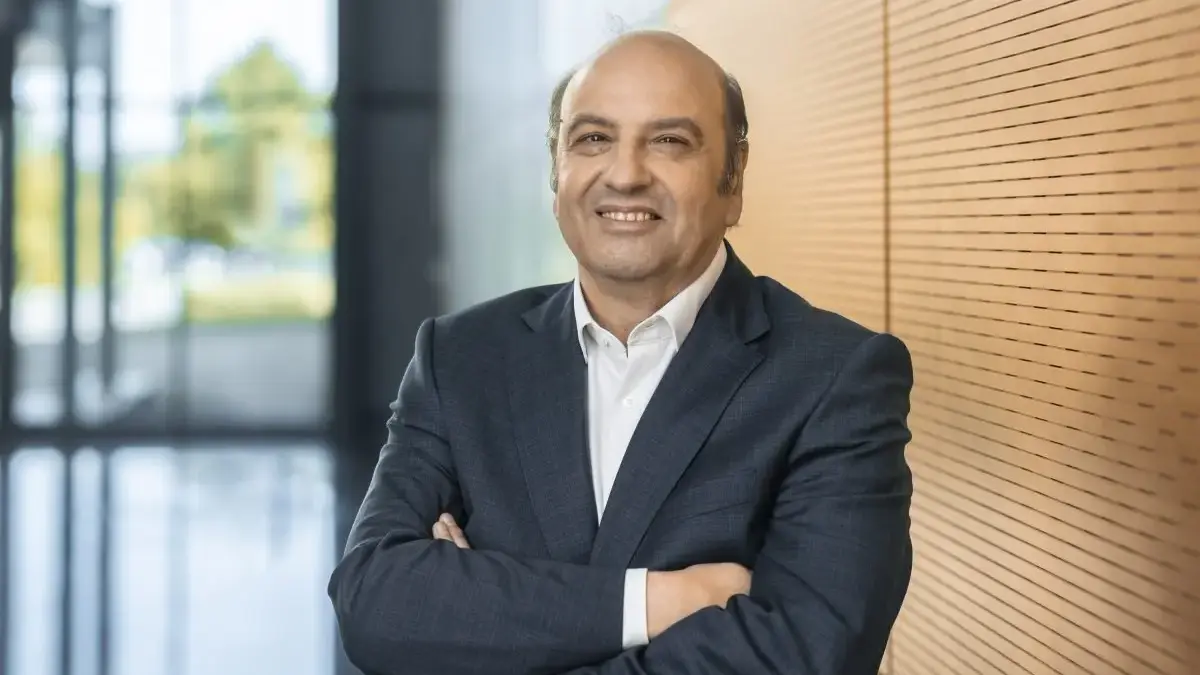
For Manfred Horstmann, senior vice president and general manager of European fabs at GlobalFoundries, the introduction of the FDX Fusion architecture directly mirrors a fundamental technological split. There is a vast chasm, he explains, between the massive, power-hungry chips required to train and run data center artificial intelligence and the agile, responsive silicon needed when intelligence physically moves out into the real world—embedded directly into cars, autonomous robots, delivery drones, heavy industrial equipment, and a wide array of edge devices.
Data center AI is exceptionally power-hungry, Horstmann noted during an exclusive interview ahead of the official global unveiling. Physical AI, by contrast, presents an entirely different class of engineering challenges. It requires far more than raw computational horsepower; it demands seamless integration with sensors, actuators, low-latency communications, ultra-low power consumption, and strict cost efficiency.
This operational philosophy underpins what GlobalFoundries describes by the acronym STAC: sense, think, act, and communicate. Rather than optimizing its silicon architecture primarily for maximum digital compute density—the traditional metric of the data center chip race—FDX Fusion is purposely engineered to combine substantial local processing power with the complex analog and mixed-signal functions required for a machine to safely and intelligently interact with its physical environment.
From FD-SOI to FDX Fusion
To understand the engineering leap behind FDX Fusion, it helps to examine the underlying architecture. FDX represents GlobalFoundries’ commercial implementation of FD-SOI technology. In this setup, the transistor channel is constructed within an extremely thin silicon film—measuring roughly 70 angstroms, or 7 nanometers—positioned directly above a buried oxide layer. Because this silicon layer is exceptionally thin, the underlying channel remains inherently fully depleted during operation. Engineers do not have to waste valuable electrical energy actively depleting the channel, which yields significant efficiency gains.
This specialized structural design grants FDX many of the advanced electrostatic performance advantages typically associated with complex FinFET architectures, but without requiring manufacturers to physically construct vertical fins on the silicon wafer. A tremendous amount of core functionality comes directly from the specialized substrate itself, eliminating the need to build a physical fin to achieve a fully depleted transistor.
GlobalFoundries is currently developing this advanced strained-silicon substrate in close collaboration with industrial and research partners CEA-Leti and Soitec. The joint development effort is part of a broader European collaborative project that Horstmann identified as Fast and FAMES. Together, these partners have already established a dedicated pilot manufacturing line in France to produce the substrate. The material utilizes a strained 70-angstrom silicon film specifically designed to boost electron mobility by approximately 25%. According to Horstmann, this collaborative framework directly builds upon the foundational success of the same European consortium that previously partnered with GlobalFoundries on its earlier 22FDX technology node.
This novel substrate forms a cornerstone of GlobalFoundries’ engineering strategy to achieve true 7-nanometer-class performance levels, but it accomplishes this feat utilizing a significantly simpler manufacturing process flow than what is typically mandatory for advanced FinFET technologies. For 7-nanometer-class performance, extreme ultraviolet (EUV) lithography is not required, Horstmann emphasized.
Company leadership projects that the initial FDX Fusion process will require approximately 50 manufacturing masks. This is notably streamlined when compared to the 70 to 80 masks commonly cited for advanced 2-nanometer and 3-nanometer FinFET manufacturing processes. The unique properties of the substrate provide a much simpler manufacturing process overall. Fewer required masks directly translate to reduced process complexity and fewer total opportunities to introduce microscopic defects during fabrication, which strongly supports both overall production yield and cost-effectiveness.
Rather than relying heavily on EUV equipment, GlobalFoundries plans to utilize advanced ArF immersion lithography, significantly tighter overlay control systems, and higher-precision photomasks supplied by Dresden-based mask maker AMTC.
The newest immersion lithography systems from ASML deliver substantial improvements in overlay and critical-dimension control. Furthermore, the multi-electron-beam-written masks produced by AMTC provide roughly 30% better overlay and critical-dimension margins compared to standard industry masks.
Physical AI Needs More Than Logic
This deliberate process strategy is vital because GlobalFoundries is not merely positioning FDX Fusion as a lower-cost alternative route to smaller digital transistors. Instead, the platform is intentionally crafted to combine dense digital logic with the rich suite of analog, radio frequency, memory, and high-voltage power management functions that physical AI systems routinely demand in the real world.
Designers can utilize the bulk underlying area for high-voltage and power-handling devices, while reserving the dedicated FD-SOI region for dense logic processing, Horstmann explained. This architectural division makes the physical integration of these diverse electronic functions markedly simpler for system designers.
The resulting platform is expected to combine dense digital logic with high-performance RF capabilities, robust analog and mixed-signal functions, ultra-low-leakage operation, embedded nonvolatile memory, and advanced in-memory computing capabilities. The first generation of FDX Fusion is projected to deliver true 7-nanometer-class digital performance alongside more than double the overall gate density of GlobalFoundries’ original first-generation FDX technology.
According to company projections, the platform should comfortably reach logic densities ranging from approximately 14 million to 18 million gates per square millimeter. Crucially, it will achieve this while carefully retaining the exceptional low-power profile and high-level integration characteristics that defined the legacy FDX architecture.
Maintaining the core advantages of 22FDX—specifically its extremely low operational power draw and seamless integration capabilities with physical sensors and actuators—is paramount. Extremely low power consumption is precisely what engineers need when developing mobile autonomous systems, industrial robots, and battery-powered aerial drones.
To accelerate market adoption and development, GlobalFoundries has outlined a clear timeline for the platform. The company expects to invest roughly $1 billion over the coming years into the ongoing development of FDX Fusion, a figure that includes approximately $250 million earmarked specifically for the initial capability toolset. Initial demonstrator silicon is currently targeted for early 2027, followed closely by an initial process design kit planned for mid-2027.
A Different AI Opportunity for Europe
For the European semiconductor industry, the rise of physical AI arrives against the backdrop of an uncomfortable strategic reality: a significant portion of the lucrative data center AI ecosystem is already heavily concentrated in other geographic regions. The data center AI train has already left the station, Horstmann acknowledged. However, when it comes to the vast, untapped frontier of physical AI, the global playing field remains wide open.
Europe does not necessarily need to win the identical manufacturing and architectural race that dominated the past decade of cloud computing. Physical AI distinctly rewards a balanced combination of low-power computing, environmental sensing, secure local communications, precise analog handling, and efficient power electronics. This technological blend aligns much more closely with Europe’s established, long-standing strengths in semiconductor manufacturing, automotive engineering, and industrial systems.
The city of Dresden serves as a primary industrial anchor for this regional strategy. The local ecosystem already hosts major manufacturing footprints from GlobalFoundries, Infineon, and Bosch, alongside specialized research organizations, a robust local network of equipment suppliers, and the expanding ESMC semiconductor manufacturing joint venture led by TSMC.
This local manufacturing cluster is rapidly becoming self-propelling, according to Horstmann. As the regional cluster continues to expand and mature, vital supply chain partners establish local manufacturing and inventory capacity, major equipment manufacturers maintain dedicated service engineering teams nearby, and innovative design houses are naturally drawn to the geographic hub.
Even the presence of the ESMC project, while technically a market competitor, serves to strengthen the broader local ecosystem. By substantially increasing Dresden’s overall manufacturing scale, it makes the entire region far more attractive and accessible to global equipment and material suppliers. For GlobalFoundries and its regional partners, the powerful combination of local manufacturing scale and highly differentiated process technology creates a historic window of opportunity. This represents a major opportunity for Europe to help define an entirely new global semiconductor market, Horstmann concluded, and to secure a leading position from the very start.


Leave a Reply