
DRESDEN — GlobalFoundries has officially taken the wraps off FDX Fusion at an event in Dresden, introducing a brand-new generation of its fully depleted silicon-on-insulator (FD-SOI) technology specifically engineered for the demands of physical AI. With this major platform rollout, the foundry is making a calculated bet that the next explosive phase of the semiconductor market will diverge significantly from the data center-focused graphics processing unit (GPU) race that has dominated the technology landscape in recent years.
Announced alongside the symbolic topping-off ceremony for SPRINT—GlobalFoundries’ major Dresden fab expansion supported by the European Chips Act—FDX Fusion represents a strategic pivot toward machines and systems that must sense, decide, communicate, and act rather than simply crunch massive computational data sets. The first generation of the technology is projected to deliver 7-nm-class digital performance, boasting more than twice the logic density of GlobalFoundries’ original FDX technology platform. Furthermore, it is designed to seamlessly integrate a broad array of critical capabilities, including radio frequency (RF), analog, mixed-signal, embedded nonvolatile memory, and in-memory computing.
To bring this vision to fruition, GlobalFoundries expects to invest roughly $1 billion over the coming years into the development of FDX Fusion. This substantial financial commitment includes approximately $250 million earmarked for the initial capability toolset. According to the company’s roadmap, demonstrator silicon is targeted for early 2027, with the initial process design kit scheduled to roll out by mid-2027. The SPRINT project itself is steadily adding vital cleanroom, laboratory, and manufacturing capacity to the Dresden site, which GlobalFoundries plans to leverage exclusively for differentiated semiconductor technologies.
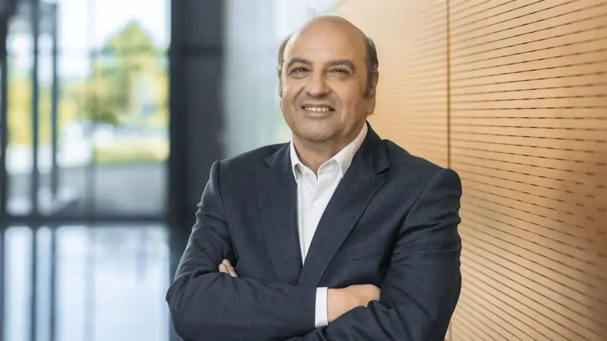
For Manfred Horstmann, senior vice president and general manager of European fabs at GlobalFoundries, the FDX Fusion architecture embodies a fundamental architectural divergence between the microchips required for centralized data center artificial intelligence and those necessitated when artificial intelligence migrates directly into vehicles, autonomous robots, drones, industrial machinery, and other edge systems.
"Data center AI is extremely power hungry," Horstmann explained during an exclusive interview prior to the public announcement. "Physical AI is a different class of problem—and it needs more than compute. It needs sensors, actuators, communications, low power, and cost efficiency."
This operational philosophy underpins what GlobalFoundries refers to as the STAC framework: sense, think, act, and communicate. Rather than optimizing chip architecture primarily for maximum digital compute density, FDX Fusion is intentionally crafted to combine substantial processing power with the comprehensive array of functions required for an autonomous machine to actively interact with its physical environment.
From FD-SOI to FDX Fusion
To understand the engineering leap behind FDX Fusion, it helps to examine the underlying physics of GlobalFoundries’ proprietary FD-SOI implementation. In standard FDX architectures, the transistor channel sits within an extremely thin silicon film—measuring approximately 70 angstroms, or 7 nanometers—positioned directly above a buried oxide layer. Because this silicon layer is exceptionally thin, the transistor channel is inherently fully depleted at all times.
"You don’t have to waste energy depleting the channel," Horstmann noted, highlighting the inherent operational efficiency of the design.
This structural characteristic provides FDX with many of the advanced electrostatic advantages typically associated with FinFET technologies, but without requiring the intricate and costly manufacturing steps necessary to construct a physical fin. "A lot of the functionality comes from the substrate itself," Horstmann added. "So we don’t need to build a fin to get a fully depleted transistor."
To develop the advanced strained-silicon substrate required for this next-generation platform, GlobalFoundries has partnered closely with research institution CEA-Leti and specialized substrate manufacturer Soitec. The collaborative effort is part of a broader European initiative identified by Horstmann as the "Fast and FAMES" project. The partners have already successfully established a pilot line in France dedicated to producing the substrate, which utilizes a strained 70-angstrom silicon film engineered to boost electron mobility by approximately 25%. Horstmann pointed out that this ongoing collaboration builds upon the exact same foundational consortium that previously partnered with GlobalFoundries on the successful 22FDX platform.
This specialized substrate forms a cornerstone of GlobalFoundries’ engineering strategy to achieve 7-nm-class performance metrics while utilizing a significantly simpler process flow than traditional, highly complex advanced FinFET technologies. "For 7-nm-class performance, we don’t need EUV," Horstmann asserted, referring to extreme ultraviolet lithography machines that carry immense capital expenditure requirements.
Instead, GlobalFoundries projects that the initial FDX Fusion process will require roughly 50 lithography masks. This stands in stark contrast to the 70 to 80 masks typically cited by industry experts for advanced 2-nm and 3-nm FinFET manufacturing processes. "The substrate gives us a much simpler process," he said, emphasizing that fewer masks directly reduce overall process complexity and substantially lower the number of potential opportunities to introduce manufacturing defects, which in turn supports both production yield and long-term cost efficiency.
Rather than relying heavily on EUV, GlobalFoundries plans to deploy advanced ArF immersion lithography, tighter overlay control systems, and higher-precision photomasks sourced from Dresden-based mask manufacturer AMTC. Horstmann noted that the newest immersion systems from ASML deliver substantial enhancements in overlay and critical-dimension control, while AMTC’s advanced multi-electron-beam-written masks provide roughly 30% better overlay and critical-dimension margins compared to standard industry masks.
Physical AI Needs More Than Logic
This deliberate process strategy is vital because GlobalFoundries is not positioning FDX Fusion merely as a lower-cost pathway to shrink digital transistors. The platform is strategically designed to combine dense digital logic with the diverse analog, radio frequency, memory, and power management functions that modern physical AI systems inherently demand.
"You can use the bulk area for high-voltage devices, and the FD-SOI area for dense logic," Horstmann explained. "That makes integrating these different functions much simpler."
According to the company’s technical roadmap, FDX Fusion will successfully combine dense digital logic with high-performance RF capabilities, analog and mixed-signal functions, low-leakage operation modes, embedded nonvolatile memory, and advanced in-memory computing architectures. Furthermore, the platform is expected to achieve logic densities ranging between approximately 14 million and 18 million gates per square millimeter, all while retaining the exceptional low-power and integration hallmarks of the existing FDX architecture.
"You maintain the advantages of 22FDX—extremely low power and very good integration with sensors and actuators," Horstmann said. "Extremely low power is what you need for mobile autonomous systems and drones."
A Different AI Opportunity for Europe
For Europe’s semiconductor sector, the launch of FDX Fusion addresses an uncomfortable underlying market reality: a significant portion of the lucrative data center AI ecosystem is already heavily concentrated outside the continent.
"The data center AI train has left the station," Horstmann acknowledged. "लेकिन for physical AI, the world is still open."
His core argument is that Europe does not need to contest the exact same technological race that is currently playing out in hyperscale data centers. Physical AI naturally rewards a distinct combination of ultra-low-power computing, advanced sensing, robust communications, precision analog capabilities, and specialized power electronics—a technological profile that aligns much more closely with Europe’s established, formidable semiconductor strengths.
The manufacturing cluster centered in Dresden provides a robust industrial foundation for this long-term strategy. The region already hosts key operations for GlobalFoundries, Infineon, and Bosch, alongside world-class research organizations, a deep network of specialized equipment suppliers, and the upcoming ESMC joint venture led by TSMC.
"The cluster is becoming self-propelling," Horstmann observed. As the regional ecosystem continues to expand and mature, specialized suppliers increasingly establish local production capacity, major equipment manufacturers maintain responsive service teams nearby, and innovative design houses are naturally drawn to the geographic hub.
Even the entry of the ESMC facility into Dresden, while technically a competitor, ultimately reinforces the strength of the local ecosystem, Horstmann pointed out. By substantially increasing the overall manufacturing scale of Dresden, the region becomes vastly more attractive to global equipment and material suppliers alike. For GlobalFoundries and its regional partners, the combination of growing manufacturing scale and differentiated technology creates a wide-open strategic window.
"This is a big opportunity for Europe to define a new market," Horstmann concluded, "and to be first."


Leave a Reply