
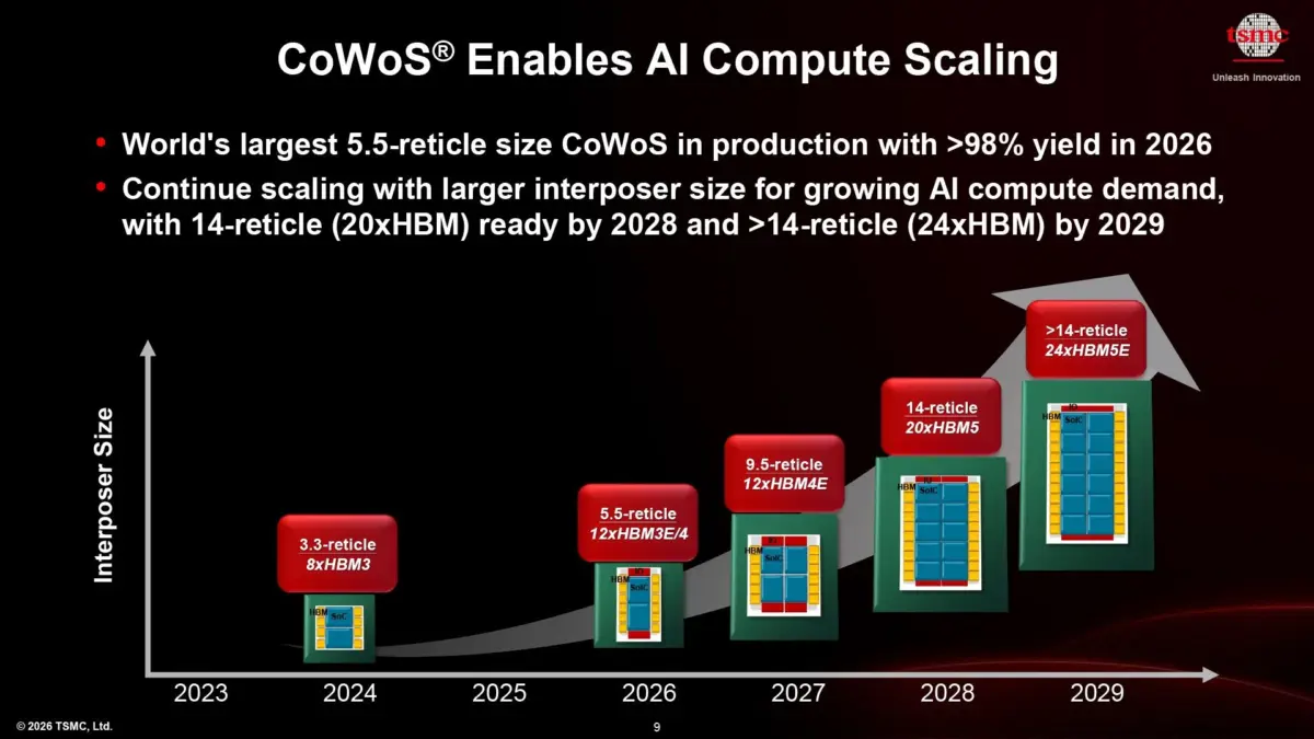
In a significant move to bolster the domestic semiconductor ecosystem, GlobalFoundries and Taiwan Semiconductor Manufacturing Company (TSMC) have entered into a major five-year manufacturing agreement valued at $2 billion. Under the terms of the new partnership, GlobalFoundries will produce silicon interposers specifically designed for TSMC’s industry-leading Chip-on-Wafer-on-Substrate (CoWoS) advanced packaging technology.
This strategic arrangement is designed to establish a reliable, U.S.-based manufacturing source for these critical components. By securing domestic production for silicon interposers—which act as the essential bridge connecting multiple logic and memory dies within an advanced package—the collaboration will enable TSMC’s diverse roster of clients to brand their finished semiconductor products as completely made and packaged within the United States. According to the current timeline outlined by the companies, volume production for the project is scheduled to ramp up significantly in the first half of 2028.
The partnership arrives at a time when the global semiconductor industry is placing an unprecedented emphasis on supply chain resilience, geographical diversification, and secure domestic manufacturing infrastructure. Advanced packaging technologies like CoWoS have become absolute bottlenecks and focal points in the production of high-performance computing hardware, artificial intelligence accelerators, and data center processors. By integrating GlobalFoundries’ established fabrication footprint in the United States into the CoWoS supply chain, the two foundry giants are directly addressing the surging demand for scalable, localized advanced packaging solutions.
Ed Kaste, senior vice president of CMOS Business at GlobalFoundries, emphasized the strategic importance of the collaboration for the broader technology sector and national manufacturing goals. Commenting on the landmark agreement, Kaste noted the value of leveraging the company’s domestic facilities to support high-end semiconductor fabrication.
"By providing manufacturing service using GF’s trusted U.S. manufacturing footprint, we are creating a secure, scalable source of essential advanced-packaging elements that will help customers accelerate innovation and strengthen the semiconductor supply chain," said Ed Kaste, senior vice president of CMOS Business at GlobalFoundries.
The inclusion of a domestic silicon interposer supplier marks a critical milestone for fabless chip designers and major technology companies that rely on TSMC’s advanced packaging prowess. Traditionally, the complex ecosystem required to build, assemble, and package cutting-edge processors has been heavily concentrated in Asian markets, particularly Taiwan. While foundries have made strides in building out front-end wafer fabrication facilities in the United States through various legislative initiatives and private investments, the lack of robust domestic advanced packaging capabilities has remained a missing puzzle piece in achieving a truly self-sufficient American semiconductor supply chain.
Silicon interposers are foundational to modern high-performance architectures, particularly those utilized in generative artificial intelligence hardware, graphics processing units, and high-end networking chips. These interposers allow multiple chiplets—such as processor cores and high-bandwidth memory stacks—to sit side-by-side on a single silicon base, communicating at high speeds with minimal latency. Without a reliable supply of interposers, the final assembly of these sophisticated processors cannot take place, making them just as crucial to the manufacturing pipeline as the lithography tools used to print microscopic transistors onto silicon wafers.
By anchoring this part of the production cycle within GlobalFoundries’ U.S. fabrication facilities, the multi-year partnership effectively bridges the gap between front-end wafer fabrication and back-end advanced packaging on American soil. This capability will prove vital for defense contractors, hyperscale cloud providers, and enterprise technology firms that face stringent compliance requirements regarding the geographic origin of their hardware components. The ability to market finished semiconductors as entirely made and packaged within the United States is expected to drive strong demand from customers operating in aerospace, defense, and critical infrastructure sectors.
As the industry looks ahead to the targeted volume production ramp-up in the first half of 2028, both GlobalFoundries and TSMC will spend the intervening years preparing their respective facilities, qualifying processes, and aligning engineering pipelines to ensure a seamless integration of operations. The $2 billion commitment underscores the long-term financial and strategic gravity of the venture, signaling a deepening cooperation between major foundry operators to tackle the complex engineering hurdles of the post-Moore’s Law era, where packaging innovation is just as important as transistor scaling.


Leave a Reply