
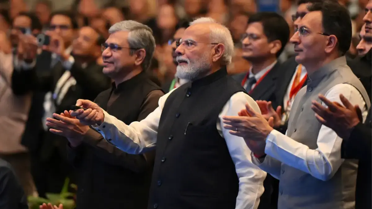
Twelve months ago, the atmosphere at SEMICON India was defined by ink drying on ceremonial memoranda of understanding. At this year’s edition, however, the narrative shifted decisively from aspirations to active industrial output. Indian Prime Minister Narendra Modi took to the stage to announce that India now officially boasts five chip assembly and packaging plants in commercial production, marking a critical milestone in the nation’s unfolding semiconductor journey. Alongside this operational breakthrough, Prime Minister Modi reiterated a formidable financial commitment of $13.5 billion for the second phase of the India Semiconductor Mission, widely known as ISM 2.0, designed to aggressively build out a comprehensive domestic semiconductor ecosystem.
A careful look at the government’s own metrics reveals that all five operational facilities are back-end units—specifically, assembly, test, marking, and packaging (ATMP) lines, rather than front-end wafer fabs. India’s long-awaited first commercial wafer fab, a major 300-mm facility spearheaded by Tata Electronics in Dholera, Gujarat, remains under active construction. Addressing these realities, Union Electronics and IT Minister Ashwini Vaishnaw explained that ISM 2.0 is specifically engineered to look beyond individual manufacturing plants. The overarching goal is to cultivate robust domestic capacity across design, equipment, specialized materials, advanced packaging, applied research and development, and specialized talent pools to support the physical hardware being manufactured.
During the high-profile event, Prime Minister Modi virtually inaugurated two brand-new production lines: CDIL Semiconductor’s facility in Mohali, Punjab, dedicated to discrete devices, and Suchi Semicon’s plant in Surat, Gujarat, focused on advanced packaging. These newly minted operations join established players like Micron, Kaynes Semicon, and CG Semi, bringing the total number of approved projects under the first phase of the semiconductor mission to 12. Highlighting immediate commercial traction, Micron CEO Sanjay Mehrotra confirmed that commercial production of DRAM and NAND memory chips is now fully underway at the company’s massive facility in Sanand, Gujarat. Adding to the momentum, Suchi Semicon and eInfochips publicly exchanged their first batch of commercial devices, celebrated as India’s inaugural commercial QFN chip.
The commercial footprint of these domestic lines is already extending far beyond national borders. Minister Vaishnaw noted that local output is actively being exported to global markets. ATMP units are currently shipping finished components to Japan, while Indian-made devices are also being seamlessly incorporated into broader technological products exported to United States and European Union destinations, including Switzerland and Germany.
Financial backing for the next phase of the national mission is scaling up significantly. Prime Minister Modi placed the total allocation for ISM 2.0 at $13.5 billion, representing a substantial increase from the approximately $8 billion earmarked during the inaugural phase. In a parallel update, Minister Vaishnaw revealed that private industry players have already made firm investment commitments amounting to roughly ₹1 lakh crore, translating to roughly $11 billion to $12 billion under the broader ecosystem program. Government projections indicate that these capital deployments will create close to 100,000 high-tech jobs over the next two to three years as corporations secure formal board and shareholder approvals. For the time being, however, these figures represent corporate commitments and strategic intents rather than immediate capital expenditure.

Building Beyond Fabs
The strategic framework of ISM 2.0 rests firmly upon six foundational pillars: comprehensive chip design, advanced machines and raw materials, more front-end fabs, a thriving ATMP and outsourced semiconductor assembly and test (OSAT) industry, applied R&D, and deep talent acquisition.
In the realm of chip design, the government has set an ambitious target of nurturing 200 dedicated chip design startups. During the first phase of the mission, 105 startups were granted access to critical electronic design automation (EDA) tools, resulting in 20 of those enterprises successfully raising venture capital funding. Furthermore, approximately 70,000 design engineers have been thoroughly trained over the past four years, marking strong progress against an original target of 85,000 engineers over a 10-year horizon. Minister Vaishnaw characterized this startup-focused push as a complete game-changer for cultivating homegrown intellectual property, noting that government skilling initiatives will now actively expand from traditional chip design toward broader system-level design methodologies.
This domestic design push operates in tandem with an already expansive semiconductor engineering base in India that routinely services major global customers. Ameer Saithu, executive vice president and global head of the Semiconductor Business Unit at HCLTech, shared insights into how major engineering firms operate within the region. He noted that the company routinely handles end-to-end semiconductor engineering—spanning from register-transfer level (RTL) design all the way through to post-silicon validation—entirely within India for multinational clients.
According to Saithu, most of the complex capabilities required to take a chip concept from initial specification to final physical parts are now firmly anchored in India. Nevertheless, he emphasized that the company continues to leverage a deeply integrated global partnership ecosystem spanning the United States, Taiwan, Malaysia, Japan, and other technology hubs. Saithu also pointed out that India is rapidly developing advanced capabilities in technical areas that were historically concentrated solely in overseas manufacturing centers. He highlighted front-end design competencies and pointed to HCLTech’s Advanced Semiconductor Lab in Bengaluru as a prime example of domestic infrastructure that provides capabilities companies previously had to source exclusively from Taiwan or Malaysia.
This industrial expansion is rippling outward, attracting major global equipment and materials corporations to position themselves directly around the manufacturing projects currently rising across the Indian landscape. Applied Materials made headlines by announcing "India Vision 2035," a strategic $5 billion investment plan slated over the coming decade aimed at achieving a tenfold expansion of its India-based supply chain capacity. Meanwhile, Lam Research confirmed plans to invest approximately ₹10,000 crore, or roughly $1.05 billion, to establish its first silicon component and vertical ingot processing plant in the country. Tokyo Electron announced intentions to open a specialized training center in Gujarat next year, and lithography giant ASML confirmed it is actively evaluating Indian suppliers to integrate into its global supply chain network.

On the manufacturing front, Tata Electronics has secured critical memoranda of understanding with premier specialty materials and industrial gas suppliers, including Fujifilm, JSR, Sumitomo Chemical, and INOX Air Products. These agreements accompany a dedicated 363-acre vendor park currently planned for development at the Dholera site.
Perhaps the most concrete development on the fab front is Tata Electronics’ partnership with Nexperia. Under the arrangement, Tata will lay the foundational groundwork to manufacture Nexperia’s advanced MOSFET product portfolio at the Dholera fab, while concurrently handling the assembly and test of Nexperia’s discrete semiconductor products at Jagiroad in Assam. While neither corporation disclosed specific production volumes, strict timelines, or financial valuations, Tata Electronics CEO Randhir Thakur confirmed that construction schedules at both strategic sites remain entirely on track, with the company pegging the combined investment at $14 billion.
AI Drives Custom Silicon Demand
Prime Minister Modi explicitly framed the strategic imperatives of ISM 2.0 around the explosive, global surge in artificial intelligence-driven semiconductor demand. He pointed out that contemporary engineering challenges now revolve around bringing memory closer to the processor, interconnecting vast arrays of distinct chips to function seamlessly as a single unified system, transferring massive data loads instantly without latency, and expertly managing complex thermal and power constraints. Furthermore, Modi underscored national energy security as a paramount prerequisite for modern chip manufacturing, pointing out that India’s installed solar capacity has experienced a massive expansion, growing from roughly 2 gigawatts to more than 160 gigawatts.
Echoing these observations from an industry perspective, HCLTech’s Saithu explained that artificial intelligence is fueling an unprecedented wave of specialized chip development. This surging demand originates not only from traditional, established semiconductor companies but also from enterprise customers who historically purchased off-the-shelf components and now require proprietary, custom-built silicon architectures.
In the AI sector, there is an immediate, urgent need for a wide variety of highly specialized chips to be engineered from the ground up, Saithu noted, explaining that his organization acts as a trusted technical partner for clients seeking to navigate this complex development cycle. He highlighted that companies across industries face immense pressure regarding time-to-market, which remains a primary operational focus for engineering service providers. Whether through enhanced technical capabilities, specialized software solutions, or AI-driven acceleration of the traditional silicon development lifecycle, service providers are working to compress time-to-market metrics for their clientele.

To address these very challenges, HCLTech developed AI Force.Semi, a specialized iteration of its core AI Force platform tailored explicitly for the semiconductor value chain. According to Saithu, the platform covers every stage of production from initial RTL design to GDSII layout and rigorous post-silicon validation, with the explicit objective of leveraging artificial intelligence to reduce cycle times, minimize engineering effort, and systematically manage technical risks across the manufacturing workflow.
This rising demand mirrors the broader expansion of India’s deep-tech and startup ecosystem. The India Deep Tech Alliance, which was launched at the previous year’s SEMICON India conference backed by $1 billion in venture capital pledges, has officially deployed $263 million across 56 promising early-stage companies. Additionally, Minister Vaishnaw revealed that an unnamed commercial fab scheduled to commence active production by 2028 has already successfully booked a massive share of its anticipated manufacturing capacity well in advance. While officials highlighted 10 approved projects a year ago, that approved roster has now expanded to 12 distinct ventures, with five already up and running.
Expanding India’s Chip Development Capabilities
This sweeping industrial build-out is generating an intense domestic demand for sophisticated engineering capabilities situated further along the complex semiconductor development lifecycle. Advanced engineering, precision testing, specialized equipment, chemical materials, targeted training programs, and applied research facilities are rapidly coalescing around the core manufacturing hubs. Concurrently, domestic firms are expanding high-end technical services that historically required access to specialized facilities located outside of India’s borders.
HCLTech’s Advanced Semiconductor Lab in Bengaluru stands out as a prime manifestation of this trend. The firm has invested approximately ₹185 crore, equivalent to roughly $19.3 million, into the cutting-edge facility. The laboratory is engineered to support early-stage prototyping and new product introduction processes, encompassing comprehensive silicon characterization, hardware validation, and rigorous reliability testing across every tier from raw wafers to fully assembled systems.
Describing the facility as a true production lab deeply integrated into the overarching engineering workflow, Saithu confirmed that the space is already actively delivering functional chips directly to the commercial market. The facility serves critical engineering and research functions, including rigorous sample-volume testing before designs are cleared for mass production. Having opened its doors just weeks prior to the event, the laboratory has already onboarded its initial cohort of commercial customers, with physical space and operational capabilities continuing to scale rapidly.

Having these advanced prototyping and testing resources physically located in India fundamentally transforms project logistics. Previously, HCLTech relied on external partners and overseas facilities situated in regions like Taiwan and Malaysia to execute similar validation tasks. Having these capabilities domestically collapses cycle times dramatically, helping us meet our customers’ demanding time-to-market requirements in a much more efficient manner, Saithu observed. Furthermore, he noted that the presence of such accessible local infrastructure provides immense strategic relief to domestic hardware startups, which historically faced prohibitive costs and logistical roadblocks when attempting to access comparable validation services abroad.
Human capital development remains an equally vital pillar of the national strategy. Saithu highlighted that HCLTech has established structured training pipelines, partnering proactively with universities across India to help shape modern curricula, mentor engineering students, and directly recruit top-tier talent into the workforce. He added that the next logical evolutionary phase for India’s engineering sector lies in advancing high-level product management and systems-level thinking in silicon architecture. While foundational front-end design competencies are firmly established, the ecosystem is poised for even broader scaling.
The three-day SEMICON India conference, hosted at the Yashobhoomi convention center in New Delhi, served as a powerful physical testament to this momentum, drawing together more than 600 participating corporations hailing from 52 distinct countries. Organizers reported a strong turnout, recording 51,656 total registrations and a cumulative footfall of approximately 40,000 visitors over the course of the three-day exhibition. By the time the final sessions concluded, event coordinators tallied 41 separate memoranda of understanding and major announcements during the opening days, complemented by an additional 15 strategic disclosures during the closing session on September 19, sealing a landmark year for India’s ambitions as a rising global semiconductor powerhouse.

Leave a Reply