
GlobalFoundries has officially unveiled FDX Fusion at its facility in Dresden, Germany, introducing a brand-new generation of its fully depleted silicon-on-insulator (FD-SOI) technology explicitly tailored for the burgeoning market of physical artificial intelligence. With this multi-million-dollar bet, the semiconductor manufacturer is signaling its belief that the next massive wave of semiconductor demand will diverge significantly from the data center-focused graphics processing unit (GPU) race that currently dominates the industry.
The announcement, delivered on October 9, coincides with the celebration of the topping-off of SPRINT, GlobalFoundries’ major Dresden fab expansion supported under the umbrella of the European Chips Act. The SPRINT project is systematically augmenting cleanroom, laboratory, and manufacturing capacity at the German site, which the company intends to leverage heavily for specialized, differentiated semiconductor manufacturing technologies moving forward.
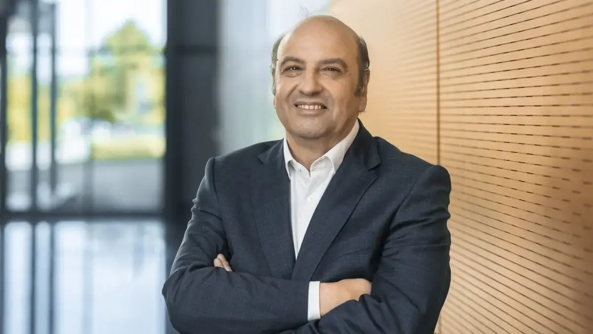
According to Manfred Horstmann, senior vice president and general manager of European fabs at GlobalFoundries, the introduction of the FDX Fusion architecture underscores a fundamental architectural schism. There is a widening gap between the massive processors required to train and run data center AI models and the specialized chips needed when intelligence is embedded directly into physical entities such as vehicles, autonomous robots, delivery drones, and industrial machinery.
“Data center AI is extremely power hungry,” Horstmann explained during an exclusive pre-announcement interview. “Physical AI is a different class of problem—and it needs more than compute. It needs sensors, actuators, communications, low power, and cost efficiency.”
This philosophy anchors what GlobalFoundries describes as the STAC paradigm: sense, think, act, and communicate. Rather than optimizing chip designs purely for maximum digital compute density, the FDX Fusion platform is engineered from the ground up to integrate substantial processing capabilities alongside the diverse array of functions a machine requires to interact seamlessly with its surrounding physical environment.
The first generation of FDX Fusion is projected to deliver 7-nm-class digital performance while achieving more than twice the transistor density of GlobalFoundries’ original FDX technology generation. Furthermore, the platform aims to tightly combine radio frequency (RF), analog, mixed-signal capabilities, embedded nonvolatile memory, in-memory computing, and dense logic onto a single piece of silicon.
To bring this vision to market, GlobalFoundries anticipates investing approximately $1 billion over the coming years dedicated entirely to FDX Fusion development. This capital expenditure envelope includes roughly $250 million earmarked specifically for the initial capability toolset. Current milestones place demonstrator silicon targets in early 2027, with an initial process design kit scheduled to follow in the middle of that same year.
From FD-SOI to FDX Fusion
To understand why GlobalFoundries believes its approach can disrupt traditional manufacturing paradigms, one must look at the mechanics of FD-SOI technology. Standard FDX implementations feature a transistor channel sitting within a remarkably thin silicon film—measuring approximately 70 angstroms, or 7 nanometers—positioned directly above a buried oxide layer. Because this silicon layer is so exceptionally thin, the channel is inherently fully depleted at all times.
“You don’t have to waste energy depleting the channel,” Horstmann noted.
This unique structural characteristic grants FDX many of the electrostatic performance advantages typically associated with complex FinFET architectures, but without the extreme manufacturing complexity of constructing physical fins. “A lot of the functionality comes from the substrate itself,” Horstmann added. “So we don’t need to build a fin to get a fully depleted transistor.”
The development of this advanced strained-silicon substrate is being spearheaded through a collaborative European research initiative—identified by Horstmann as the “Fast and FAMES” project—which pairs GlobalFoundries with research institutions CEA-Leti and wafer specialist Soitec. Together, the partners have already established a dedicated pilot line in France focused on the substrate. The material utilizes a strained 70-angstrom silicon film designed explicitly to boost electron mobility by roughly 25%. Horstmann pointed out that this ongoing collaboration builds upon the same trusted consortium that previously partnered with GlobalFoundries on its 22FDX platform.
This novel substrate is a cornerstone of the company’s strategy to achieve 7-nm-class performance metrics utilizing a significantly simpler process flow than what is required by contemporary advanced FinFET nodes. “For 7-nm-class performance, we don’t need EUV,” Horstmann stated, referencing extreme ultraviolet lithography machines, which carry immense capital costs.
GlobalFoundries estimates that the initial FDX Fusion process will require roughly 50 masks. In stark contrast, Horstmann cited that advanced 2-nm and 3-nm FinFET processes typically demand between 70 and 80 masks. “The substrate gives us a much simpler process,” he said, emphasizing that fewer masks inherently reduce process complexity, lower the number of potential points of failure or defects, and ultimately support both superior manufacturing yields and reduced production costs.
Instead of relying on EUV, GlobalFoundries plans to deploy advanced ArF immersion lithography, tighter overlay control protocols, and higher-precision photomasks sourced from Dresden-based mask maker AMTC. According to Horstmann, the newest immersion systems from ASML deliver substantial enhancements in overlay and critical-dimension control, while multi-electron-beam-written masks from AMTC provide roughly 30% better overlay and critical-dimension margins compared to standard commercial masks.
Physical AI Needs More Than Logic
This deliberate process strategy is vital because GlobalFoundries is deliberately avoiding positioning FDX Fusion merely as a lower-cost path toward shrinking digital transistors. Instead, the entire platform is conceptualized to merge ultra-dense logic with the wide array of analog, RF, memory, and power-management functions that modern physical AI systems cannot live without.
“You can use the bulk area for high-voltage devices, and the FD-SOI area for dense logic,” Horstmann explained. “That makes integrating these different functions much simpler.”
The company projects that FDX Fusion will achieve logic densities spanning roughly 14 million to 18 million gates per square millimeter, while simultaneously preserving the ultra-low-power profile and integration versatility that defined the foundational FDX architecture.
“You maintain the advantages of 22FDX—extremely low power and very good integration with sensors and actuators,” he said. “Extremely low power is what you need for mobile autonomous systems and drones.”
A Different AI Opportunity for Europe
The unveiling of FDX Fusion also highlights a pragmatic approach to Europe’s position in the global semiconductor landscape. Europe faces a distinct structural reality when it comes to artificial intelligence hardware: the vast majority of the data center AI ecosystem and its supply chains are already heavily concentrated in other parts of the world.
“The data center AI train has left the station,” Horstmann acknowledged. “But for physical AI, the world is still open.”
His central argument is that Europe has no architectural or economic necessity to contest the same high-power data center race. Physical AI inherently rewards a synthesis of low-power compute, edge sensing, robust communications, precision analog handling, and efficient power electronics—a matrix of technical requirements that aligns much more closely with Europe’s existing, deeply rooted semiconductor strengths and industrial infrastructure.
Dresden itself serves as a vital anchor for this localized strategy. The regional cluster already hosts major manufacturing footprints from GlobalFoundries, Infineon, and Bosch, alongside elite research organizations, specialized equipment suppliers, and the emerging ESMC joint venture led by TSMC.
“The cluster is becoming self-propelling,” Horstmann observed. As the regional ecosystem continues to expand and densify, more specialized suppliers establish local operational capacity, international equipment makers maintain dedicated service teams nearby, and growing design houses are naturally drawn to the geographic hub. Even the establishment of ESMC in the region, despite being a commercial competitor, ultimately reinforces the broader ecosystem by multiplying Dresden’s overall manufacturing scale and rendering the local supply chain drastically more attractive to global vendors.
For GlobalFoundries, the confluence of expanding local manufacturing scale and uniquely tailored process technology represents a golden window of opportunity. It allows the company to stake an early claim in a market that is only beginning to take shape.
“This is a big opportunity for Europe to define a new market,” Horstmann concluded, “and to be first.”


Leave a Reply