
In early September, Apple officially introduced the iPhone Duo, marking the Cupertino-based tech giant’s long-anticipated entry into the foldable smartphone segment. While Apple’s debut drew global attention, the foldable market is far from a nascent space; competitors such as Samsung and Huawei have spent years refining flexible device form factors, pushing the envelope with innovative designs including advanced tri-fold models.
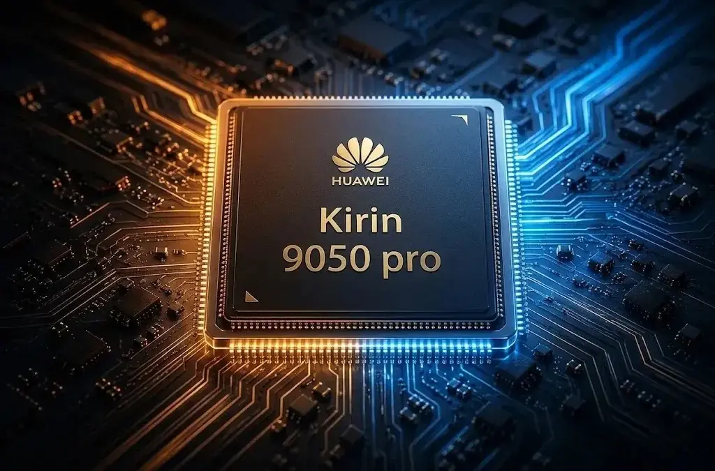
Huawei continues to command headlines in this arena, not merely for the physical engineering of its hardware, but for the breakthrough silicon powering its latest flagship. Alongside the release of the Huawei Mate XT 2 Ultimate Design tri-fold smartphone, the company has introduced its proprietary Kirin 9050 Pro processor. Referred to in earlier technical documents as “Kirin 2026,” this new system-on-chip operationalizes Huawei’s Tau ($tau$) Scaling Law. The foundational concept was formally unveiled by He Tingbo, president of Huawei’s semiconductor unit, during the 2026 IEEE International Symposium on Circuits and Systems.
Faced with stringent export controls and restricted access to advanced extreme ultraviolet (EUV) lithography equipment from ASML, Huawei has been forced to pioneer alternative architectural pathways. Rather than relying on traditional horizontal shrinkage to boost performance, the company has engineered a novel design approach known as LogicFolding. This technique vertically stacks active silicon layers on top of one another, effectively shortening signal routing paths while dramatically increasing overall transistor density.
From Spatial Geometry to Temporal Scaling
For decades, the semiconductor industry has relied on the tenets of Moore’s Law, driving computational gains by aggressively shrinking transistor dimensions. However, in the absence of advanced EUV lithography tools, traditional scaling methods introduce severe physical limitations. As physical wires become thinner, electrical resistance and parasitic capacitance increase, inadvertently slowing down chip performance and compounding thermal dissipation challenges.

By shifting the engineering focus from spatial geometry to temporal performance, Huawei’s LogicFolding technique directly addresses these timing constraints. The methodology revolutionizes digital, analog, and memory circuits across vertically stacked silicon tiers by replacing lengthy horizontal interconnects with short, vertical channels. According to technical data released by Huawei, this vertical stacking architecture successfully reduces core routing lengths by 20% and shortens key timing paths by an impressive 70%.
This architectural shift also provides a crucial remedy for thermal management issues. Because data transmission across traditional horizontal copper wires accounts for more than 80% of a modern processor’s total energy consumption, shortening these signal paths drastically curtails power draw. Measurements cited by TrendForce and EE Times China demonstrate that power consumption plummeted by 66% for the neural processing unit, 58% for the graphics processing unit, and 41% for the CPU cores when running at comparable performance levels. To keep operating temperatures manageable, Huawei has opted to strategically lower operating voltages and clock speeds rather than pushing them higher through brute force.
Achieving such intricate three-dimensional active layers, however, introduces formidable engineering and economic hurdles. Mateo Valero, director of the Barcelona Supercomputing Center (BSC), highlighted these systemic realities in an interview with EE Times. As traditional silicon scaling approaches fundamental physical boundaries, Valero noted that isolated transistor-level innovations are no longer sufficient on their own.
"The transistor is important, but what matters now is how an entire system behaves," Valero said, emphasizing that modern computational success depends entirely on full-stack orchestration. "You have to co-design from the application all the way down to the transistor, software, system-on-chip architecture, and memory layout, or you run into bottlenecks elsewhere."
Consumer Deployment and the Global Performance Gap
The tangible result of these semiconductor advancements is embodied in the Huawei Mate XT 2 Ultimate Design. Priced from 19,999 yuan (approximately $2,980) up to 24,999 yuan (roughly $3,725), the high-end tri-fold smartphone officially hit shelves on September 12, though its commercial availability remains strictly confined to the Chinese domestic market.

Underneath its flexible exterior, the Mate XT 2 is powered by the Kirin 9050 Pro. The processor features a robust nine-core CPU architecture, anchored by a primary core operating at a peak frequency of 3.1 GHz. Graphics are handled by a Maleoon 920 GPU capable of supporting hardware-accelerated ray tracing at up to 50 million rays per second. Furthermore, the chip integrates a powerful Da Vinci neural processing unit designed to run a 30-billion-parameter Mixture-of-Experts artificial intelligence model directly on the device without relying on cloud infrastructure.
Manufacturing Realities, Foundry Friction, and Economic Cost
Despite its impressive performance benchmarks, the manufacturing reality behind LogicFolding involves extreme fabrication complexity. Domestic foundry partner SMIC has previously demonstrated the capability to produce 7-nm-class chips without EUV lithography, and industry analysts believe the Kirin 9050 Pro utilizes a comparable manufacturing process, though Huawei has not officially disclosed the exact foundry or node specifications.
The chip’s packaging architecture incorporates two active logic layers alongside a 1.5-micron hybrid-bonding pitch. This configuration establishes approximately 50 million vertical connections, with roughly 10% to 15% actively carrying live signals. Looking ahead, Huawei reports that its subsequent Kirin 2027 test silicon has already successfully reduced the hybrid-bonding pitch down to 1 micron, featuring over 100 million vertical interconnects. The company’s roadmap outlines an ambitious goal to achieve a 720-nm pitch over the next three years, culminating by 2031 in a transistor density equivalent to a commercial 1.4-nm process.
Nevertheless, manufacturing yields remain a persistent vulnerability when active logic layers are connected directly. The fabrication process demands hyper-precise wafer thinning and surface planarization to eliminate microscopic gaps, while even minor misalignments of copper pads can introduce severe wiring defects and structural warping.
Weighing in on these systemic obstacles, Valero reiterated that isolated architectural tricks are ultimately insufficient. "Unless memory arrangement, compilers, and hardware scheduling are seamlessly orchestrated, isolated architectural tricks cannot overcome physical manufacturing constraints," he observed.

The financial toll of these developments is evident in Huawei’s corporate balance sheets. During the first half of the fiscal year, the company’s research and development expenditures surged 25.2% year-on-year to reach 121.38 billion yuan, equivalent to roughly $18.13 billion and accounting for 25.9% of total revenue. Concurrently, net profit fell sharply by 36% down to 23.81 billion yuan. Ongoing U.S. export restrictions have compelled Huawei to pour immense capital into achieving self-reliance across artificial intelligence and semiconductor capabilities. These escalating R&D costs, compounded by rising global memory chip prices, continue to exert heavy pressure on the company’s overall profitability and consumer electronics division.
LinxISA Versus Arm and RISC-V
In an effort to insulate its hardware ecosystem from escalating geopolitical risks, Huawei has also begun pivoting away from standard instruction set architectures. Although the firm holds a perpetual licensing agreement for the older Armv8 architecture, U.S. export regulations continue to introduce significant regulatory and supply chain vulnerabilities regarding the adoption of newer iterations like Armv9.
To circumvent these restrictions, Huawei is reportedly developing LinxISA, an innovative block-structured instruction set architecture. Unlike conventional architectures such as Arm or RISC-V that process instructions sequentially one at a time, LinxISA is designed to execute instructions in cohesive blocks. While industry observers speculate on its deployment, the explicit utilization of LinxISA within the Kirin 9050 Pro has not yet been publicly confirmed by the manufacturer.
Reiterating his perspective on holistic hardware design, Valero told EE Times that individual architectural decisions cannot be evaluated in a vacuum, noting that optimizing isolated hardware components without comprehensive system orchestration inevitably generates performance bottlenecks across the entire software and hardware stack.
Software Autonomy and Enterprise Compute Ambitions

Complementing its hardware innovations, Huawei has continued to distance its software ecosystem from Western dependencies by rolling out HarmonyOS 7. The proprietary operating system completely strips out open-source Android code, instead relying entirely on its own independently developed microkernel and enhanced read-only file system (EROFS).
Huawei’s long-term strategy extends far beyond consumer mobile devices. The company intends to deploy its LogicFolding methodology into enterprise-grade data center infrastructure. By 2030, Huawei plans to launch the Ascend 990 AI processor, positioning it as a direct domestic competitor to industry heavyweights like Nvidia and Alibaba.
Commenting on the viability of these large-scale, end-to-end integration efforts, Valero remarked that when dedicated architectural teams successfully optimize systems from top to bottom, they possess the structural foundation to build competitive platforms capable of challenging global market leaders.
To secure this vision, Huawei is actively working to cultivate a fully self-sufficient domestic semiconductor equipment supply chain. Collaborating closely with domestic partners such as AMEC and NAURA—which are actively developing specialized manufacturing tools for plasma etching, thin-film deposition, and advanced packaging—Huawei hopes to domesticate every phase of chip production, laying the groundwork for a resilient technological ecosystem in the face of persistent international trade barriers.

Leave a Reply